LM74
SPI/MICROWIRE
TM
12-Bit Plus Sign Temperature Sensor
General Description
The LM74 is a temperature sensor, Delta-Sigma analog-to-
digital converter with an SPI and MICROWIRE compatible
interface. The host can query the LM74 at any time to read
temperature. A shutdown mode decreases power consump-
tion to less than 10 µA. This mode is useful in systems where
low average power consumption is critical.
The LM74 has 12-bit plus sign temperature resolution
(0.0625∞C per LSB) while operating over a temperature
range of -55∞C to +150∞C.
The LM74's 3.0V to 5.5V supply voltage range, low supply
current and simple SPI interface make it ideal for a wide
range of applications. These include thermal management
and protection applications in hard disk drives, printers, elec-
tronic test equipment, and office electronics. The LM74 is
available in the SO-8 package as well as an 5-Bump micro
SMD package.
Applications
n
System Thermal Management
n
Personal Computers
n
Disk Drives
n
Office Electronics
n
Electronic Test Equipment
Features
n
0.0625∞C temperature resolution.
n
Shutdown mode conserves power between temperature
reading
n
SPI and MICROWIRE Bus interface
n
5-Bump micro SMD package saves space
Key Specifications
j
Supply Voltage
3.0V or 2.65V to
5.5V
j
Supply Current
operating
265µA (typ)
520µA (max)
shutdown
3µA (typ)
j
Temperature
Accuracy
-10∞C to 65∞C
±
1.25∞C(max)
-25∞C to 110∞C
±
2.1∞C(max)
-55∞C to 125∞C
±
3∞C(max)
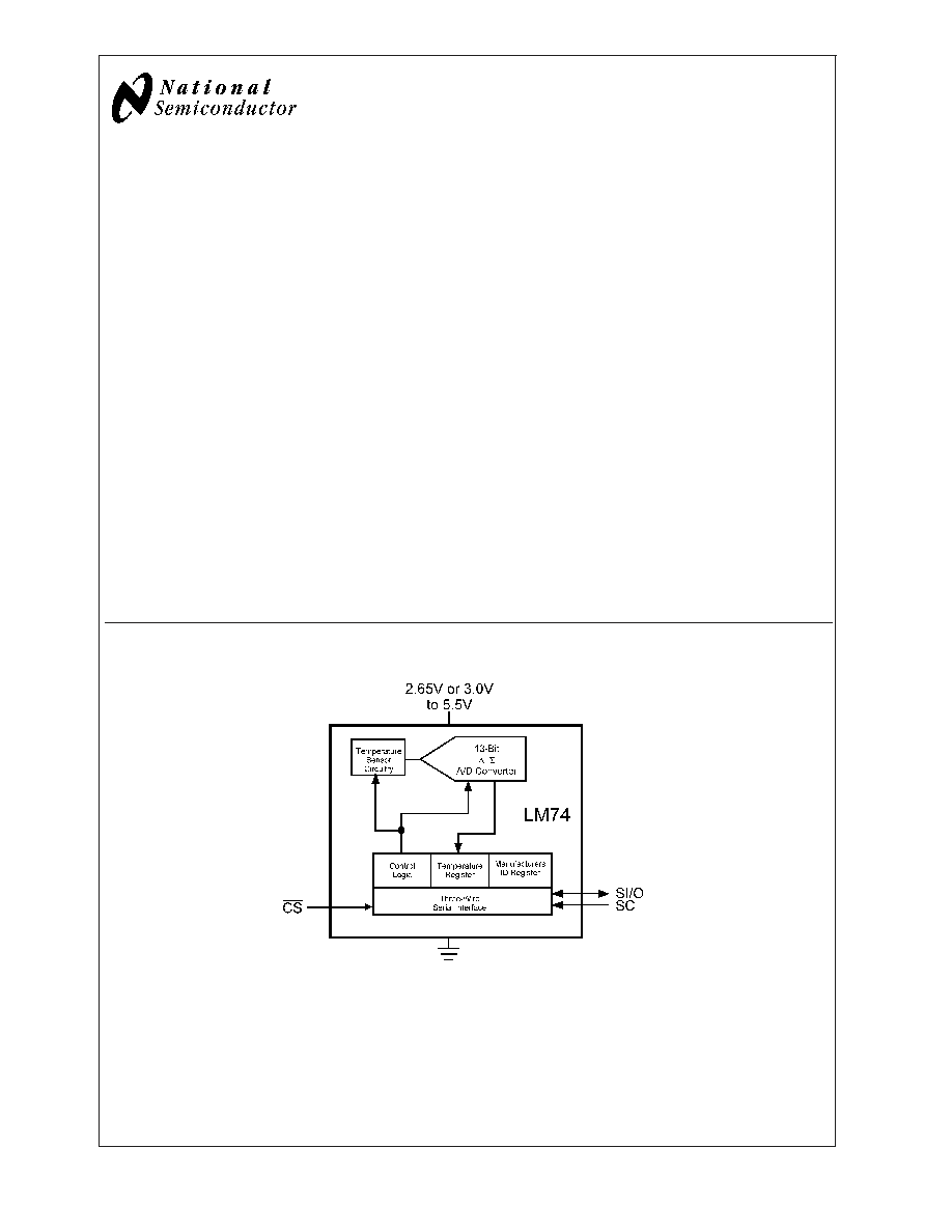
Simplified Block Diagram
10090901
MICROWIRE
Æ
is a registered trademark of National Semiconductor Corporation.
TRI-STATE
Æ
is a registered trademark of National Semiconductor Corporation.
April 2003
LM74
SPI/MICROWIRE
12-Bit
Plus
Sign
T
emperature
Sensor
© 2003 National Semiconductor Corporation
DS100909
www.national.com

Connection Diagrams
SO-8
5-Bump micro SMD
10090902
TOP VIEW
NS Package Number M08A
10090924
Note:
-
Pin numbers are referenced to the package marking text orientation. Pin
1 is designated by the square.
-
Reference JEDEC Registration MO-211, variation BC
- The top 4 characters designate the date code. The bottom 3 characters
designate the device type (see ordering information).
TOP VIEW
NS Package Number BPD05MPB
Ordering Information
Order Number
Package
Marking
NS Package
Number
Supply Voltage
Transport Media
LM74CIM-3
LM74CIM-3
SO-8, M08A
3.0V to 3.6V
95 Units in Rail
LM74CIMX-3
LM74CIM-3
SO-8, M08A
3.0V to 3.6V
2500 Units in Tape and Reel
LM74CIM-5
LM74CIM-5
SO-8, M08A
4.5V to 5.5V
95 Units in Rail
LM74CIMX-5
LM74CIM-5
SO-8, M08A
4.5V to 5.5V
2500 Units in Tape and Reel
LM74CIBP-3
T8
micro SMD,
BPD05MPB
2.65V to 3.6V
250 Units in Tape and Reel
LM74CIBPX-3
T8
micro SMD,
BPD05MPB
2.65V to 3.6V
3000 Units in Tape and Reel
LM74CIBP-5
T9
micro SMD,
BPD05MPB
4.5V to 5.5V
250 Units in Tape and Reel
LM74CIBPX-5
T9
micro SMD,
BPD05MPB
4.5V to 5.5V
3000 Units in Tape and Reel
LM74
www.national.com
2
Pin Descriptions
Label
SO-8
Pin #
micro
SMD
Pin #
Function
Typical Connection
SI/O
1
1
Slave Input/Output - Serial bus bi-directional data
line. Schmitt trigger input.
From and to Controller
SC
2
5
Slave Clock - Serial bus clock Schmitt trigger input
line.
From Controller
NC
3
No Connection
No Connection
GND
4
4
Power Supply Ground
Ground
NC
5
No Connection
No Connection
NC
6
No Connection
No Connection
CS
7
3
Chip Select input.
From Controller
V
+
8
2
Positive Supply Voltage Input
DC Voltage from 3.0V to 5.5V for the
LM74CIM and 2.65V to 5.5V for the
LM74CIBP. Bypass with a 0.1 µF ceramic
capacitor.
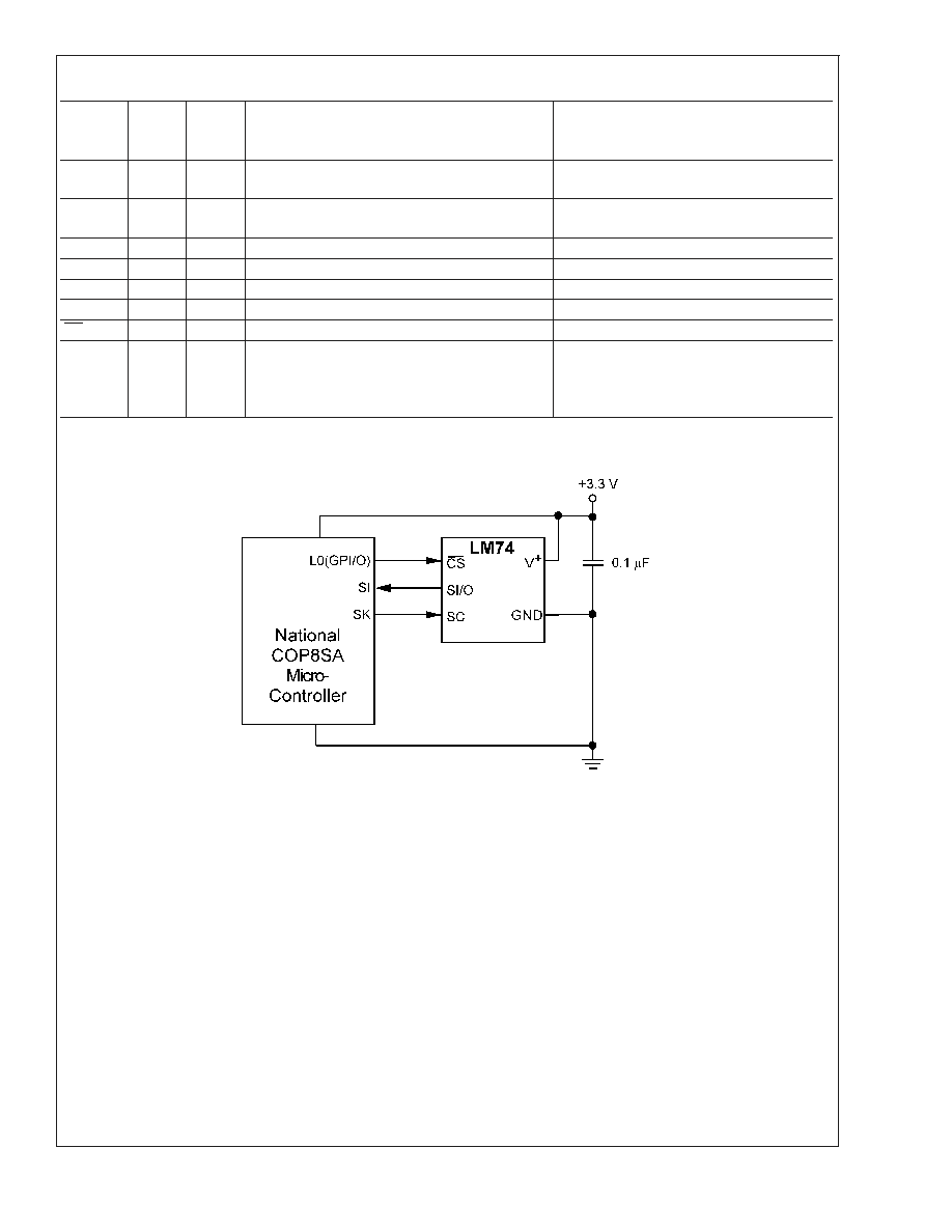
Typical Application
10090903
FIGURE 1. COP Microcontroller Interface
LM74
www.national.com
3

Absolute Maximum Ratings
(Note 1)
Supply Voltage
-0.3V to 6.0V
Voltage at any Pin
-0.3V to V
+
+ 0.3V
Input Current at any Pin (Note 2)
5 mA
Package Input Current (Note 2)
20 mA
Storage Temperature
-65∞C to +150∞C
Soldering Information, Lead Temperature
SO-8 Package (Note 3)
Vapor Phase (60 seconds)
Infrared (15 seconds)
215∞C
220∞C
ESD Susceptibility (Note 4)
Human Body Mode
LM74CIBP SC, pin 5
1900V
LM74CIM and LM74CIBP all
other pins
2000V
Machine Model
200V
Operating Ratings
Specified Temperature Range
T
MIN
to T
MAX
(Note 5)
LM74CIBP
LM74CIM
-40∞C to +125∞C
-55∞C to +150∞C
Supply Voltage Range (+V
S
)
LM74CIBP
+2.65V to +5.5V
LM74CIM
+3.0V to +5.5V
Temperature-to-Digital Converter Characteristics
Unless otherwise noted, these specifications apply for V
+
= 2.65V to 3.6V for the LM74CIBP -3, V
+
= 3.0V to 3.6V for the
LM74CIM -3 and V
+
= 4.5V to 5.5V for the LM74 -5 (Note 6). Boldface limits apply for T
A
= T
J
= T
MIN
to T
MAX
; all other lim-
its T
A
= T
J
=+25∞C, unless otherwise noted.
Parameter
Conditions
Typical
(Note 7)
LM74-5
Limits
(Note 8)
LM74-3
Limits
(Note 8)
Units
(Limit)
Temperature Error (Note 6)
T
A
= -10∞C to +65∞C
±
1.25
±
1.25
∞C (max)
T
A
= -25∞C to +110∞C
±
2.1
+2.65/-2.15
∞C (max)
T
A
= -40∞C to +85∞C
+2.65/-1.65
±
2.15
∞C (max)
T
A
= -40∞C to +110∞C
+2.65/
-2.0
+2.65/-2.15
∞C (max)
T
A
= -55∞C to +125∞C
±
3.0
±
3.5
∞C (max)
T
A
= -55∞C to +150∞C
±
5.0
±
5.0
∞C (max)
Resolution
13
Bits
Temperature
Conversion Time
SO-8
(Note 9)
280
425
425
ms (max)
micro SMD
(Note 9)
611
925
925
ms (max)
Quiescent Current
SO-8
Serial Bus Inactive
310
520
520
µA (max)
micro SMD
265
470
470
µA (max)
SO-8
Serial Bus Active
310
µA
micro SMD
310
µA
SO-8
Shutdown Mode,
V
+
= 3.3V
7
µA
micro SMD
3
µA
SO-8
Shutdown Mode,
V
+
= 5V
8
µA
micro SMD
4
µA
Logic Electrical Characteristics
DIGITAL DC CHARACTERISTICS Unless otherwise noted, these specifications apply for V
+
= 2.65V to 3.6V for the
LM74CIBP -3, V
+
= 3.0V to 3.6V for the LM74CIM -3 and V
+
= 4.5V to 5.5V for the LM74 -5 (Note 6). Boldface limits apply
for T
A
= T
J
= T
MIN
to T
MAX
; all other limits T
A
= T
J
=+25∞C, unless otherwise noted.
Symbol
Parameter
Conditions
Typical
(Note 7)
Limits
(Note 8)
Units
(Limit)
V
IN(1)
Logical "1" Input Voltage
V
+
x 0.7
V (min)
V
+
+ 0.3
V (max)
V
IN(0)
Logical "0" Input Voltage
-0.3
V (min)
V
+
x 0.3
V (max)
Input Hysteresis Voltage
V
+
= 3.0V to 3.6V
0.8
0.35
V (min)
V
+
= 4.5V to 5.5V
0.8
0.33
V (min)
I
IN(1)
Logical "1" Input Current
V
IN
= V
+
0.005
3.0
µA (max)
LM74
www.national.com
4
Logic Electrical Characteristics
(Continued)
DIGITAL DC CHARACTERISTICS Unless otherwise noted, these specifications apply for V
+
= 2.65V to 3.6V for the
LM74CIBP -3, V
+
= 3.0V to 3.6V for the LM74CIM -3 and V
+
= 4.5V to 5.5V for the LM74 -5 (Note 6). Boldface limits apply
for T
A
= T
J
= T
MIN
to T
MAX
; all other limits T
A
= T
J
=+25∞C, unless otherwise noted.
Symbol
Parameter
Conditions
Typical
(Note 7)
Limits
(Note 8)
Units
(Limit)
I
IN(0)
Logical "0" Input Current
V
IN
= 0V
-0.005
-3.0
µA (min)
C
IN
All Digital Inputs
20
pF
V
OH
High Level Output Voltage
I
OH
= -400 µA
2.4
V (min)
V
OL
Low Level Output Voltage
I
OL
= +2 mA
0.4
V (max)
I
O_TRI-STATE
TRI-STATE Output Leakage
Current
V
O
= GND
V
O
= V
+
-1
+1
µA (min)
µA
(max)
SERIAL BUS DIGITAL SWITCHING CHARACTERISTICS Unless otherwise noted, these specifications apply for V
+
= 2.65V
to 3.6V for the LM74CIBP -3, V
+
= 3.0V to 3.6V for the LM74CIM -3 and V
+
= 4.5V to 5.5V for the LM74 -5 (Note 6); C
L
(load
capacitance) on output lines = 100 pF unless otherwise specified. Boldface limits apply for T
A
= T
J
= T
MIN
to T
MAX
; all other
limits T
A
= T
J
= +25∞C, unless otherwise noted.
Symbol
Parameter
Conditions
Typical
(Note 7)
Limits
(Note 8)
Units
(Limit)
t
1
SC (Clock) Period
0.16
DC
µs (min)
(max)
t
2
CS Low to SC (Clock) High Set-Up Time
100
ns (min)
t
3
CS Low to Data Out (SO) Delay
70
ns (max)
t
4
SC (Clock) Low to Data Out (SO) Delay
100
ns (max)
t
5
CS High to Data Out (SO) TRI-STATE
200
ns (max)
t
6
SC (Clock) High to Data In (SI) Hold Time
50
ns (min)
t
7
Data In (SI) Set-Up Time to SC (Clock) High
30
ns (min)
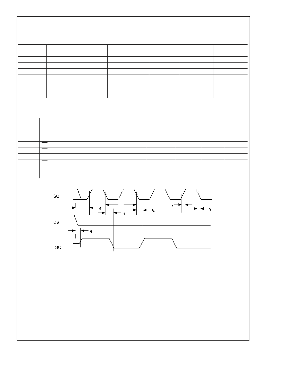
10090904
FIGURE 2. Data Output Timing Diagram
LM74
www.national.com
5

Logic Electrical Characteristics
(Continued)
Note 1: Absolute Maximum Ratings indicate limits beyond which damage to the device may occur. DC and AC electrical specifications do not apply when operating
the device beyond its rated operating conditions.
Note 2: When the input voltage (V
I
) at any pin exceeds the power supplies (V
I
<
GND or V
I
>
+V
S
) the current at that pin should be limited to 5 mA. The 20 mA
maximum package input current rating limits the number of pins that can safely exceed the power supplies with an input current of 5 mA to four.
Note 3: See AN-450 "Surface Mounting Methods and Their Effect on Product Reliability" or the section titled "Surface Mount" found in a current National
Semiconductor Linear Data Book for other methods of soldering surface mount devices.
Note 4: Human body model, 100 pF discharged through a 1.5 k
resistor. Machine model, 200 pF discharged directly into each pin.
Note 5: The life expectancy of the LM74 will be reduced when operating at elevated temperatures. LM74
JA
(thermal resistance, junction-to-ambient) when
attached to a printed circuit board with 2 oz. foil is summarized in the table below:
Device Number
NS Package
Number
Thermal
Resistance (
JA
)
LM74CIM
M08A
160∞C/W
LM74CIBP
BPD05MPB
250∞C/W
Note 6: All SOP (LM74CIM) parts will function over the V
+
supply voltage range of 3V to 5.5V. All micro SMD (LM74SIBP) parts will function over the V
+
supply
voltage range of 2.65V to 5.5V. The SOP (LM74CIM) parts are tested and specified for rated temperature error at their nominal supply voltage for temperature ranges
of -10∞C to +65∞C, -55∞C to +125∞C and -55∞C to +150∞C. For the SOP (LM74CIM) parts the temperature error specifications for temperature ranges of -40∞C to
+85∞C, -25∞C to +110∞C and -40∞C to +110∞C include error induced by power supply variation of
±
5% from the nominal value. For the LM74CIM (SOP) parts the
temperature error will increase by
±
0.3∞C for a power supply voltage (V
+
) variation of
±
10% from the nominal value.
For the LM74CIBP-3 (micro SMD) parts all accuracies are guaranteed over the supply range of 2.65V to 3.6V, except for the temperature ranges of -55∞C to 125∞C
and -55∞C to +150∞C where the accuracy applies for the nominal supply voltage of 3.3V. For the LM74CIBP-5 (micro SMD) parts all accuracies are guranteed over
the supply range of 4.75V to 5.25V, except for the temperature ranges of -55∞C to 125∞C and -55∞C to +150∞C where the accuracy applies for the nominal supply
voltage of 5.0V. For the LM74CIBP over -55∞C to 125∞C and -55∞C to +150∞C, a power supply variation of
±
10% will degrade the accuracy by
±
0.3∞C.
10090905
FIGURE 3. TRI-STATE Data Output Timing Diagram
10090906
FIGURE 4. Data Input Timing Diagram
LM74
www.national.com
6
Logic Electrical Characteristics
(Continued)
Note 7: Typicals are at T
A
= 25∞C and represent most likely parametric norm.
Note 8: Limits are guaranteed to National's AOQL (Average Outgoing Quality Level).
Note 9: This specification is provided only to indicate how often temperature data is updated. The LM74 can be read at any time without regard to conversion state
(and will yield last conversion result). A conversion in progress will not be interrupted. The output shift register will be updated at the completion of the read and a
new conversion restarted.
Note 10: For best accuracy, minimize output loading. Higher sink currents can affect sensor accuracy with internal heating. This can cause an error of 0.64∞C at full
rated sink current and saturation voltage based on junction-to-ambient thermal resistance.
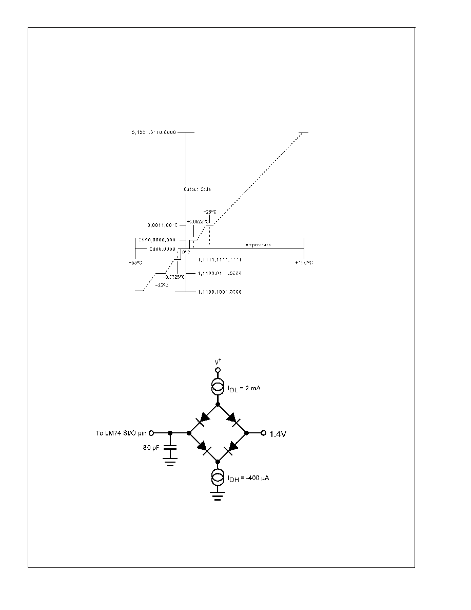
Electrical Characteristics
TRI-STATE Test Circuit
10090908
FIGURE 5. Temperature-to-Digital Transfer Function (Non-linear scale for clarity)
10090907
FIGURE 6.
LM74
www.national.com
7

Typical Performance Characteristics
Average Power-On Reset Voltage vs Temperature
Static Supply Current vs Temperature (SO-8)
10090923
10090921
Static Supply Current vs Temperature (micro SMD)
Temperature Error (SO-8)
10090925
10090922
1.0 Functional Description
The LM74 temperature sensor incorporates a band-gap type
temperature sensor and 12-bit plus sign
ADC (Delta-
Sigma Analog-to-Digital Converter). Compatibility of the
LM74's three wire serial interface with SPI and MICROWIRE
allows simple communications with common microcontrol-
lers and processors. Shutdown mode can be used to opti-
mize current drain for different applications. A Manufacture's/
Device
ID
register
identifies
the
LM74
as
National
Semiconductor product.
1.1 POWER UP AND POWER DOWN
When the supply voltage is less than about 1.6V (typical),
the LM74 is considered powered down. The LM74 always
powers up in a known state. When the supply voltage rises
above 1.6V (typical), an internal Power-On Reset (POR)
occurs and the temperature register will then contain a value
of 1111 1111 0000 00XX, where XX indicates undefined
values. See Section 1.5.2 for a diagram of the Temperature
Regisiter contents after POR but before completion of the
first temperature conversion.
The LM74 power-up default condition is continuous conver-
sion mode. After completion of the first full temperature
conversion, the register will contain temperature measure-
ment data in bits D15 (the temperature data MSB) through
D3 (the temperature data LSB). Bit D2 will be fixed high; bits
D1 and D0 are undefined. See Section 1.5.3 for a diagram of
the Temperature Regisiter contents after the first complete
temperature conversion. Note that bit D2 represents a com-
plete conversion flag. During POR it is low and, after the first
temperature conversion is complete, it goes high. This bit
can be polled to indicate when the POR data in the Tem-
perature Register has been replaced with valid temperature
data.
After the first conversion, and any subsequent conversions,
the value in the temperature register does not change until
the completion of the next conversion, at which time the
temperature register is updated with the latest temperature
value.
1.2 SERIAL BUS INTERFACE
The LM74 operates as a slave and is compatible with SPI or
MICROWIRE bus specifications. Data is clocked out on the
falling edge of the serial clock (SC), while data is clocked in
on the rising edge of SC. A complete transmit/receive com-
LM74
www.national.com
8

1.0 Functional Description
(Continued)
munication will consist of 32 serial clocks. The first 16 clocks
comprise the transmit phase of communication, while the
second 16 clocks are the receive phase.
When CS is high SI/O will be in TRI-STATE
Æ
. Communica-
tion should be initiated by taking chip select (CS) low. This
should not be done when SC is changing from a low to high
state. Once CS is low the serial I/O pin (SI/O) will transmit
the first bit of data. The master can then read this bit with the
rising edge of SC. The remainder of the data will be clocked
out by the falling edge of SC. Once the 14 bits of data (one
sign bit, twelve temperature bits and 1 high bit) are transmit-
ted the SI/O line will go into TRI-STATE. CS can be taken
high at any time during the transmit phase. If CS is brought
low in the middle of a conversion the LM74 will complete the
conversion and the output shift register will be updated after
CS is brought back high.
The receive phase of a communication starts after 16 SC
periods. CS can remain low for 32 SC cycles. The LM74 will
read the data available on the SI/O line on the rising edge of
the serial clock. Input data is to an 8-bit shift register. The
part will detect the last eight bits shifted into the register. The
receive phase can last up to 16 SC periods. All ones must be
shifted in order to place the part into shutdown. A zero in any
location will take the LM74 out of shutdown. The following
codes should only be transmitted to the LM74:
∑
00 hex
∑
01 hex
∑
03 hex
∑
07 hex
∑
0F hex
∑
1F hex
∑
3F hex
∑
7F hex
∑
FF hex
any others may place the part into a Test Mode. Test Modes
are used by National Semiconductor to thoroughly test the
function of the LM74 during production testing. Only eight
bits have been defined above since only the last eight trans-
mitted are detected by the LM74, before CS is taken HIGH.
The following communication can be used to determine the
Manufacturer's/Device ID and then immediately place the
part into continuous conversion mode. With CS continuously
low:
∑
Read 16 bits of temperature data
∑
Write 16 bits of data commanding shutdown
∑
Read 16 bits of Manufacture's/Device ID data
∑
Write 8 to 16 bits of data commanding Conversion Mode
∑
Take CS HIGH.
Note that one complete temperature conversion period will
have to pass before the LM74 Temperature register will
contain the new temperature data. Until then, it will contain a
"stale" temperature (the data that was in the register before
going into shutdown mode).
1.3 TEMPERATURE DATA FORMAT
Temperature data is represented by a 13-bit, two's comple-
ment word with an LSB (Least Significant Bit) equal to
0.0625∞C:
Temperature
Digital Output
Binary
Hex
+150∞C
0100 1011 0000 0111
4B 07h
+125∞C
0011 1110 1000 0111
3E 87h
+25∞C
0000 1100 1000 0111
0C 87h
+0.0625∞C
0000 0000 0000 1111
00 0Fh
0∞C
0000 0000 0000 0111
00 07h
-0.0625∞C
1111 1111 1111 1111
FF FFh
-25∞C
1111 0011 1000 0111
F3 87h
-55∞C
1110 0100 1000 0111
E4 87h
Note: The last two bits are TRI-STATE
Æ
and depicted as one
in the table.
The first data byte is the most significant byte with most
significant bit first, permitting only as much data as neces-
sary to be read to determine temperature condition. For
instance, if the first four bits of the temperature data indicate
an overtemperature condition, the host processor could im-
mediately take action to remedy the excessive tempera-
tures.
1.4 SHUTDOWN MODE/MANUFACTURER'S ID
Shutdown mode is enabled by writing XX FF to the LM74 as
shown in Figure 7c. The serial bus is still active when the
LM74 is in shutdown. Current draw drops to less than 10 µA
between serial communications. When in shutdown mode
the LM74 always will output 1000 0000 0000 00XX. This is
the manufacturer's/Device ID information. The first 5-bits of
the field (1000 0XXX) are reserved for manufacturer's ID. As
mentioned in Section 1.2, writing a zero to the LM74 con-
figuration register will take it out of shutdown mode and
place it in conversion mode. In other words, any valid code
listed in Section 1.2 other than XX FF will put it in conversion
mode. After leaving shutdown, but before the first tempera-
ture conversion is complete, the temperature register will
contain the last measured temperature which resided in the
temperature register before entering shutdown mode. After
the completion of the first conversion, the temperature reg-
ister will be updated with the new temperature data.
LM74
www.national.com
9

1.0 Functional Description
(Continued)
1.5 INTERNAL REGISTER STRUCTURE
The LM74 has three registers, the temperature register, the
configuration register and the manufacturer's/device identifi-
cation register. The temperature and manufacturer's/device
identification registers are read only. The configuration reg-
ister is write only.
1.5.1 Configuration Register
(Selects shutdown or continuous conversion modes):
(Write Only):
D15
D14
D13
D12
D11
D10
D9
D8
D7
D6
D5
D4
D3
D2
D1
D0
X
X
X
X
X
X
X
X
Shutdown
D0≠D15 set to XX FF hex enables shutdown mode.
D0≠D15 set to 00 00 hex sets Continuous conversion mode.
Note: setting D0-D15 to any other values may place the LM74 into a manufacturer's test mode, upon which the LM74 will stop
responding as described. These test modes are to be used for National Semiconductor production testing only. See Section 1.2
Serial Bus Interface for a complete discussion.
1.5.2 Temperature Register (after power-up, before first complete temperature conversion)
(Read Only):
D15
D14
D13
D12
D11
D10
D9
D8
D7
D6
D5
D4
D3
D2
D1
D0
1
1
1
1
1
1
1
1
0
0
0
0
0
0
X
X
D0≠D1: Undefined. TRI-STATE will be output on SI/0.
D2≠D15: Power-on Reset (POR) values.
1.5.3 Temperature Register (after completion of first temperature conversion)
(Read Only):
D15
D14
D13
D12
D11
D10
D9
D8
D7
D6
D5
D4
D3
D2
D1
D0
MSB
Bit 11
Bit 10
Bit 9
Bit 8
Bit 7
Bit 6
Bit 5
Bit 4
Bit 3
Bit 2
Bit 1
LSB
1
X
X
D0≠D1: Undefined. TRI-STATE will be output on SI/0.
D2: High.
D3≠D15: Temperature Data. One LSB = 0.0625∞C. Two's complement format.
1.5.4 Manufacturer's Device ID Register
(Read Only):
D15
D14
D13
D12
D11
D10
D9
D8
D7
D6
D5
D4
D3
D2
D1
D0
1
0
0
0
0
0
0
0
0
0
0
0
0
0
X
X
D0≠D1: Undefined. TRI-STATE will be output on SI/0.
D2≠D15: Manufacturer's/Device ID Data. This register is accessed whenever the LM74 is in shutdown mode.
LM74
www.national.com
10
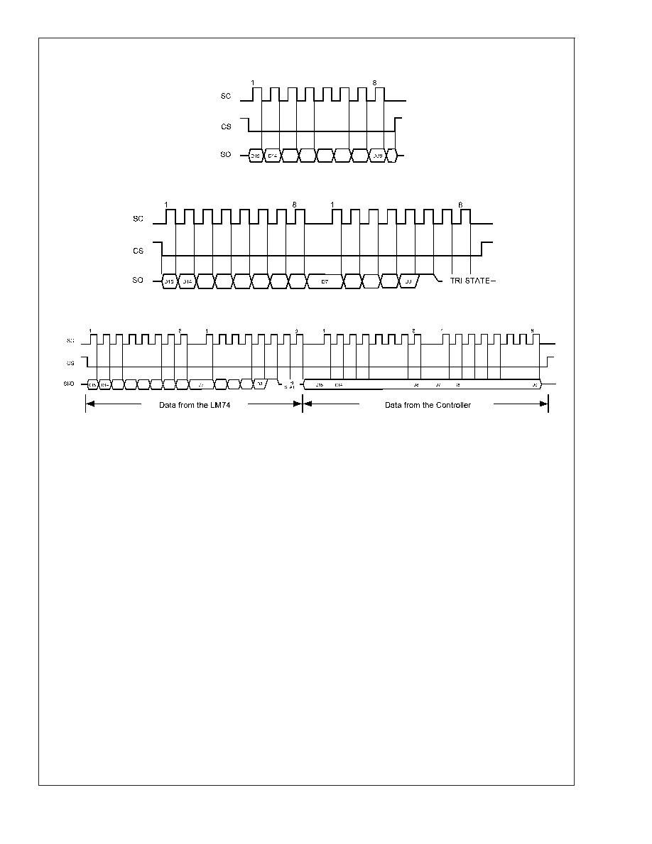
2.0 Serial Bus Timing Diagrams
10090914
a) Reading Continuous Conversion - Single Eight-Bit Frame
10090915
b) Reading Continuous Conversion - Two Eight-Bit Frames
10090918
c) Writing Shutdown Control
FIGURE 7. Timing Diagrams
LM74
www.national.com
11

3.0 Application Hints
To get the expected results when measuring temperature
with an integrated circuit temperature sensor like the LM74,
it is important to understand that the sensor measures its
own die temperature. For the LM74, the best thermal path
between the die and the outside world is through the LM74's
pins. In the SO-8 package all the pins on the LM74 will have
an equal effect on the die temperature. Because the pins
represent a good thermal path to the LM74 die, the LM74 will
provide an accurate measurement of the temperature of the
printed circuit board on which it is mounted. There is a less
efficient thermal path between the plastic package and the
LM74 die. If the ambient air temperature is significantly
different from the printed circuit board temperature, it will
have a small effect on the measured temperature.
In probe-type applications, the LM74 can be mounted inside
a sealed-end metal tube, and can then be dipped into a bath
or screwed into a threaded hole in a tank. As with any IC, the
LM74 and accompanying wiring and circuits must be kept
insulated and dry, to avoid leakage and corrosion. This is
especially true if the circuit may operate at cold temperatures
where condensation can occur. Printed-circuit coatings and
varnishes such as Humiseal and epoxy paints or dips are
often used to insure that moisture cannot corrode the LM74
or its connections.
3.1 micro SMD LIGHT SENSITIVITY
The LM74 in the micro SMD package should not be exposed
to ultraviolet light. The micro SMD package does not com-
pletely encapsulate the LM74 die in epoxy. Exposing the
LM74 micro SMD package to bright sunlight will not imme-
diatly cause a change in the output reading. Our experi-
ments show that directly exposing the circuit side (bump
side) of the die to high intensity (
1mW/cm
2
) ultraviolet light,
centered at a wavelength of 254nm, for greater than 20
minutes will deprogram the EEPROM cells in the LM74.
Since the EEPROM is used for storing calibration coeffi-
cients, the LM74 will function but the temperature accuracy
will no longer be as specified. Light can penetrate through
the side of the package as well, so exposure to ultra violet
radiation is not recommended even after mounting.
4.0 Typical Applications
10090920
FIGURE 8. Temperature monitor using Intel 196 processor
LM74
www.national.com
12

4.0 Typical Applications
(Continued)
10090919
FIGURE 9. LM74 digital input control using micro-controller's general purpose I/O.
LM74
www.national.com
13

Physical Dimensions
inches (millimeters) unless otherwise noted
8-Lead Molded Small Outline Package
Order Number LM74CIM-3, LM74CIMX-3, LM74CIM-5 or LM74CIMX-5
NS Package Number M08A
5-Bump micro SMD Ball Grid Array Package
Order Number LM74CIBP-3,LM74CIBPX-3, LM74CIBP-5, LM74CIBPX-5
NS Package Number BPD05MPB
The following dimensions apply to the BPD05MPB package
shown above: X1=1565µm
±
30µm, X2=1615µm
±
30µm, X3=850µm
±
50µm.
LM74
www.national.com
14

Notes
LIFE SUPPORT POLICY
NATIONAL'S PRODUCTS ARE NOT AUTHORIZED FOR USE AS CRITICAL COMPONENTS IN LIFE SUPPORT
DEVICES OR SYSTEMS WITHOUT THE EXPRESS WRITTEN APPROVAL OF THE PRESIDENT AND GENERAL
COUNSEL OF NATIONAL SEMICONDUCTOR CORPORATION. As used herein:
1. Life support devices or systems are devices or
systems which, (a) are intended for surgical implant
into the body, or (b) support or sustain life, and
whose failure to perform when properly used in
accordance with instructions for use provided in the
labeling, can be reasonably expected to result in a
significant injury to the user.
2. A critical component is any component of a life
support device or system whose failure to perform
can be reasonably expected to cause the failure of
the life support device or system, or to affect its
safety or effectiveness.
BANNED SUBSTANCE COMPLIANCE
National Semiconductor certifies that the products and packing materials meet the provisions of the Customer Products
Stewardship Specification (CSP-9-111C2) and the Banned Substances and Materials of Interest Specification
(CSP-9-111S2) and contain no ``Banned Substances'' as defined in CSP-9-111S2.
National Semiconductor
Americas Customer
Support Center
Email: new.feedback@nsc.com
Tel: 1-800-272-9959
National Semiconductor
Europe Customer Support Center
Fax: +49 (0) 180-530 85 86
Email: europe.support@nsc.com
Deutsch Tel: +49 (0) 69 9508 6208
English
Tel: +44 (0) 870 24 0 2171
FranÁais Tel: +33 (0) 1 41 91 8790
National Semiconductor
Asia Pacific Customer
Support Center
Email: ap.support@nsc.com
National Semiconductor
Japan Customer Support Center
Fax: 81-3-5639-7507
Email: jpn.feedback@nsc.com
Tel: 81-3-5639-7560
www.national.com
LM74
SPI/MICROWIRE
12-Bit
Plus
Sign
T
emperature
Sensor
National does not assume any responsibility for use of any circuitry described, no circuit patent licenses are implied and National reserves the right at any time without notice to change said circuitry and specifications.