 | –≠–ª–µ–∫—Ç—Ä–æ–Ω–Ω—ã–π –∫–æ–º–ø–æ–Ω–µ–Ω—Ç: LM760H | –°–∫–∞—á–∞—Ç—å:  PDF PDF  ZIP ZIP |

TL H 10067
LM760
High
Speed
Differential
Comparator
December 1994
LM760
High Speed Differential Comparator
General Description
The LM760 is a differential voltage comparator offering con-
siderable speed improvement over the LM710 family and
operates from symmetric supplies of
g
4 5V to
g
6 5V The
LM760 can be used in high speed analog-to-digital conver-
sion systems and as a zero crossing detector in disc file and
tape amplifiers The LM760 output features balanced rise
and fall times for minimum skew and close matching be-
tween the complementary outputs The outputs are TTL
compatible with a minimum sink capability of two gate loads
Features
Y
Guaranteed high speed
25 ns response time
Y
Guaranteed delay matching on both outputs
Y
Complementary TTL compatible outputs
Y
High sensitivity
Y
Standard supply voltages
Applications
Y
High speed A-to-D
Y
Peak or zero detector
Connection Diagram
8-Lead DIP
TL H 10067 ≠ 3
Top View
Ordering Information
Temperature Range
NSC
Commercial
Package Type
Package
0 C to
a
70 C
Drawing
LM760CN
8-lead Plastic DIP
N08E
C1995 National Semiconductor Corporation
RRD-B30M115 Printed in U S A
Absolute Maximum Ratings
If Military Aerospace specified devices are required
please contact the National Semiconductor Sales
Office Distributors for availability and specifications
Storage Temperature Range
Metal Can and Ceramic DIP
b
65 C to
a
175 C
Molded DIP
b
65 C to
a
150 C
Operating Temperature Range
Military (LM760)
b
55 C to
a
125 C
Commercial (LM760C)
0 C to
a
70 C
Lead Temperature
Metal Can and Ceramic DIP
(Soldering 60 sec )
300 C
Molded DIP (Soldering 10 sec )
265 C
Positive Supply Voltage
a
8 0V
Negative Supply Voltage
b
8 0V
Peak Output Current
10 mA
Differential Input Voltage
g
5 0V
Input Voltage
V
a t
V
I
t
V
b
ESD Susceptibility
TBD
LM760
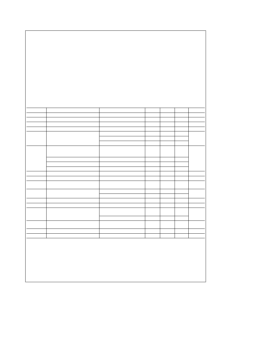
Electrical Characteristics
V
CC
e
g
4 5V to
g
6 5V T
A
e b
55 C to
a
125 C T
A
e
25 C for typical figures unless otherwise specified
Symbol
Parameter
Conditions
Min
Typ
Max
Units
V
IO
Input Offset Voltage
R
S
s
200X
1 0
6 0
mV
I
IO
Input Offset Current
0 5
7 5
m
A
I
IB
Input Bias Current
8 0
60
m
A
R
O
Output Resistance (Either Output)
V
O
e
V
OH
100
X
t
PD
Response Time
T
A
e
25 C (Note 3)
18
30
T
A
e
25 C (Note 4)
25
ns
(Note 5)
16
D
t
PD
Response Time Difference
between Outputs (Note 1)
(t
PD
of
a
V
I1
)
b
(t
PD
of
b
V
I2
)
T
A
e
25 C
5 0
(t
PD
of
a
V
I2
)
b
(t
PD
of
b
V
I1
)
T
A
e
25 C
5 0
ns
(t
PD
of
a
V
I1
)
b
(t
PD
of
a
V
I2
)
T
A
e
25 C
7 5
(t
PD
of
b
V
I1
)
b
(t
PD
of
b
V
I2
)
T
A
e
25 C
7 5
R
I
Input Resistance
f
e
1 0 MHz
12
kX
C
I
Input Capacitance
f
e
1 0 MHz
8 0
pF
D
V
IO
D
T
Average Temperature Coefficient
R
S
e
50X
3 0
m
V C
of Input Offset Voltage
T
A
e b
55 C to
a
125 C
D
I
IO
D
T
Average Temperature Coefficient
T
A
e a
25 C to
a
125 C
2 0
nA C
of Input Offset Current
T
A
e a
25 C to
b
55 C
7 0
V
IR
Input Voltage Range
V
CC
e
g
6 5V
g
4 0
g
4 5
V
V
IDR
Differential Input Voltage Range
g
5 0
V
V
OH
Output Voltage HIGH
0 mA
s
I
OH
s
5 0 mA
2 4
3 2
(Either Output)
V
CC
e a
5 0V
V
I
OH
e
80 mA V
CC
e
g
4 5V
2 4
3 0
V
OL
Output Voltage LOW
I
OL
e
3 2 mA
0 25
0 4
V
(Either Output)
I
a
Positive Supply Current
V
CC
e
g
6 5V
18
32
mA
I
b
Negative Supply Current
V
CC
e
g
6 5V
9 0
16
mA
2

LM760C
Electrical Characteristics
V
CC
e
g
4 5V to
g
6 5V T
A
e
0 C to
a
70 C T
A
e
25 C for typical figures unless otherwise specified
Symbol
Parameter
Conditions
Min
Typ
Max
Units
V
IO
Input Offset Voltage
R
S
s
200X
1 0
6 0
mV
I
IO
Input Offset Current
0 5
7 5
m
A
I
IB
Input Bias Current
8 0
60
m
A
R
O
Output Resistance (Either Output)
V
O
e
V
OH
100
X
t
PD
Response Time
T
A
e
25 C (Note 3)
18
30
T
A
e
25 C (Note 4)
25
ns
(Note 5)
16
D
t
PD
Response Time Difference
between Outputs (Note 1)
(t
PD
of
a
V
I1
)
b
(t
PD
of
b
V
I2
)
T
A
e
25 C
5 0
(t
PD
of
a
V
I2
)
b
(t
PD
of
b
V
I1
)
T
A
e
25 C
5 0
ns
(t
PD
of
a
V
I1
)
b
(t
PD
of
a
V
I2
)
T
A
e
25 C
10
(t
PD
of
b
V
I1
)
b
(t
PD
of
b
V
I2
)
T
A
e
25 C
10
R
I
Input Resistance
f
e
1 0 MHz
12
kX
C
I
Input Capacitance
f
e
1 0 MHz
8 0
pF
D
V
IO
D
T
Average Temperature Coefficient
R
S
e
50X
3 0
m
V C
of Input Offset Voltage
T
A
e
0 C to
a
70 C
D
I
IO
D
T
Average Temperature Coefficient
T
A
e a
25 C to
a
70 C
5 0
nA C
of Input Offset Current
T
A
e a
25 C to 0 C
10
V
IR
Input Voltage Range
V
CC
e
g
6 5V
g
4 0
g
4 5
V
V
IDR
Differential Input Voltage Range
g
5 0
V
V
OH
Output Voltage HIGH
0 mA
s
I
OH
s
5 0 mA
2 4
3 2
(Either Output)
V
CC
e a
5 0V
V
I
OH
e
80 mA V
CC
e
g
4 5V
2 5
3 0
V
OL
Output Voltage LOW
I
OL
e
3 2 mA
0 25
0 4
V
(Either Output)
I
a
Positive Supply Current
V
CC
e
g
6 5V
18
34
mA
I
b
Negative Supply Current
V
CC
e
g
6 5V
9 0
16
mA
Note 1
T
J Max
e
150 C
Note 2
Ratings apply to ambient temperature at 25 C
Note 3
Response time measured from the 50% point of a 30 mV
P≠P
10 MHz sinusoidal input to the 50% point of the output
Note 4
Response time measured from the 50% point of a 2 0 V
P≠P
10 MHz sinusoidal input to the 50% point of the output
Note 5
Response time measured from the start of a 100 mV input step with 5 0 mV overdrive to the time when the output crosses the logic threshold
3

Typical Performance Characteristics
Various Output Overdrives
Response Time for
Various Input Overdrives
Response Time for
Input Voltage
Response Time vs
Input Voltage
Response Time vs
Characteristic
Voltage Transfer
Characteristic
Voltage Transfer
Supply Voltage
Voltage Gain vs
vs Temperature
Voltage Gain
vs Temperature
Input Bias Current
vs Temperature
Input Offset Current
vs Temperature
Response Time
vs Temperature
Output Voltage Levels
TL H 10067 ≠ 5
4
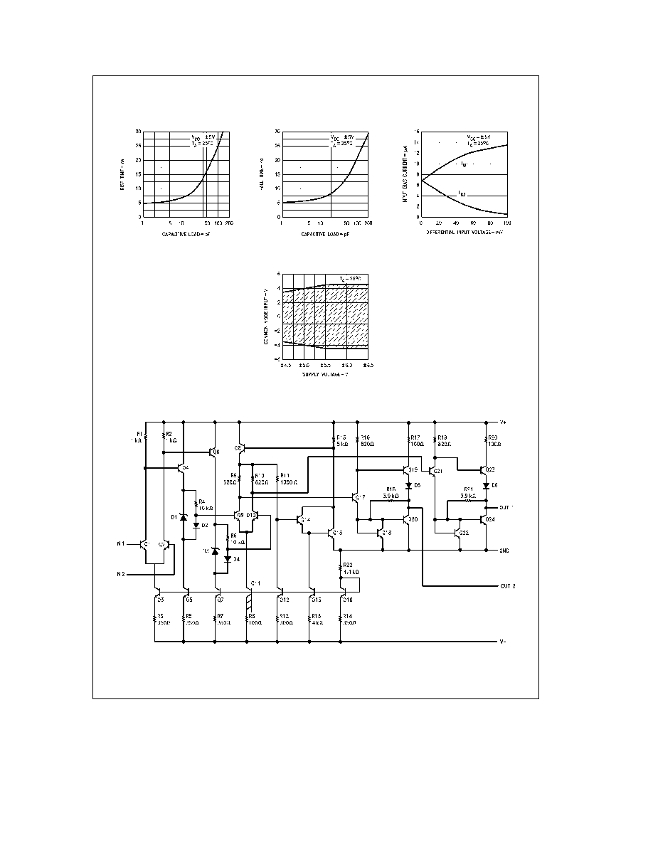
Typical Performance Characteristics
(Continued)
Capacitive Load
Rise Time vs
Capacitive Load
Fall Time vs
Differential Input Voltage
Input Bias Current vs
vs Supply Voltage
Common Mode Range
TL H 10067 ≠ 6
Equivalent Circuit
TL H 10067 ≠ 4
5