 | ÐлекÑÑоннÑй компоненÑ: LM8262MMX | СкаÑаÑÑ:  PDF PDF  ZIP ZIP |
Äîêóìåíòàöèÿ è îïèñàíèÿ www.docs.chipfind.ru
LM8262 Dual
RRIO, High Output Current & Unlimited Cap Load Op
Amp in MSOP
General Description
The LM8262 is a Rail-to-Rail input and output Op Amp which
can operate with a wide supply voltage range. This device
has high output current drive, greater than Rail-to-Rail input
common mode voltage range, unlimited capacitive load drive
capability, and provides tested and guaranteed high speed
and slew rate. It is specifically designed to handle the re-
quirements of flat panel TFT panel V
COM
driver applications
as well as being suitable for other low power, and medium
speed applications which require ease of use and enhanced
performance over existing devices.
Greater than Rail-to-Rail input common mode voltage range
with 50dB of Common Mode Rejection, allows high side and
low side sensing, among many applications, without having
any concerns over exceeding the range and no compromise
in accuracy. In addition, most device parameters are insen-
sitive to power supply variations; this design enhancement is
yet another step in simplifying its usage. The output stage
has low distortion (0.05% THD+N) and can supply a respect-
able amount of current (15mA) with minimal headroom from
either rail (300mV).
The LM8262 is offered in the space saving MSOP package.
Features
(V
S
= 5V, T
A
= 25°C, Typical values unless specified).
n
GBWP
21MHz
n
Wide supply voltage range
2.5V to 22V
n
Slew rate
12V/µs
n
Supply current/channel
1.15 mA
n
Cap load limit
Unlimited
n
Output short circuit current
+53mA/-75mA
n
+/-5% Settling time
400ns (500pF, 100mV
PP
step)
n
Input common mode voltage
0.3V beyond rails
n
Input voltage noise
15nV/
n
Input current noise
1pA/
n
THD+N
<
0.05%
Applications
n
TFT-LCD flat panel V
COM
driver
n
A/D converter buffer
n
High side/low side sensing
n
Headphone amplifier
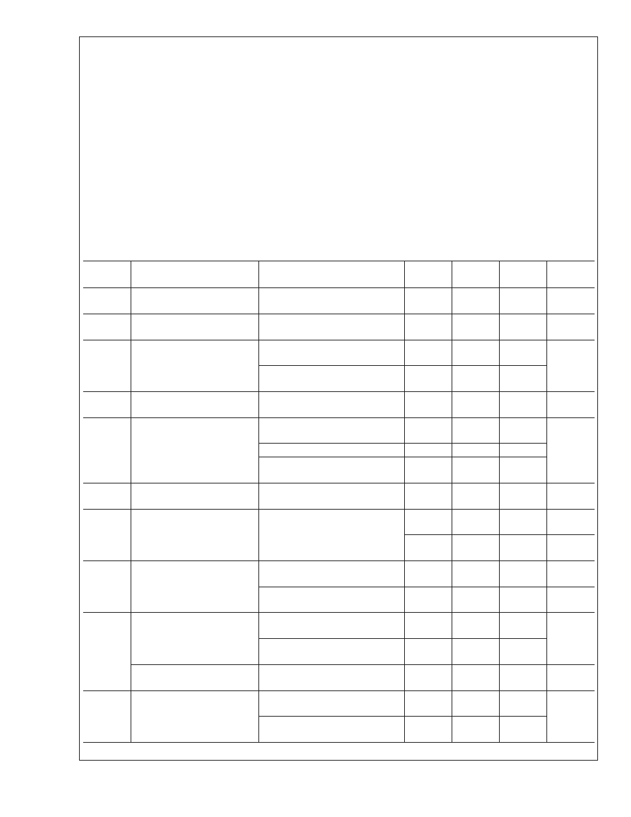
Output Response with Heavy Capacitive Load
20021037
Connection Diagram
8-Pin MSOP
20021001
Top View
Ordering Information
Package
Part Number
Package
Marking
Media Transport
NSC Drawing
8-Pin MSOP
LM8262MM
A46
1k Units Tape and Reel
MUA08A
LM8262MMX
3.5k Units Tape and Reel
June 2002
LM8262
Dual
RRIO,
High
Output
Current
&
Unlimited
Cap
Load
Op
Amp
in
MSOP
© 2002 National Semiconductor Corporation
DS200210
www.national.com
Absolute Maximum Ratings
(Note 1)
If Military/Aerospace specified devices are required,
please contact the National Semiconductor Sales Office/
Distributors for availability and specifications.
ESD Tolerance
2KV (Note 2)
200V(Note 9)
V
IN
Differential
+/-10V
Output Short Circuit Duration
(Notes 3, 11)
Supply Voltage (V
+
- V
-
)
24V
Voltage at Input/Output pins
V
+
+0.8V, V
-
-0.8V
Storage Temperature Range
-65°C to +150°C
Junction Temperature (Note 4)
+150°C
Soldering Information:
Infrared or Convection (20 sec.)
235°C
Wave Soldering (10 sec.)
260°C
Operating Ratings
Supply Voltage (V
+
- V
-
)
2.5V to 22V
Junction Temperature Range(Note 4)
-40°C to +85°C
Package Thermal Resistance,
JA
,(Note 4)
8-Pin MSOP
235°C/W
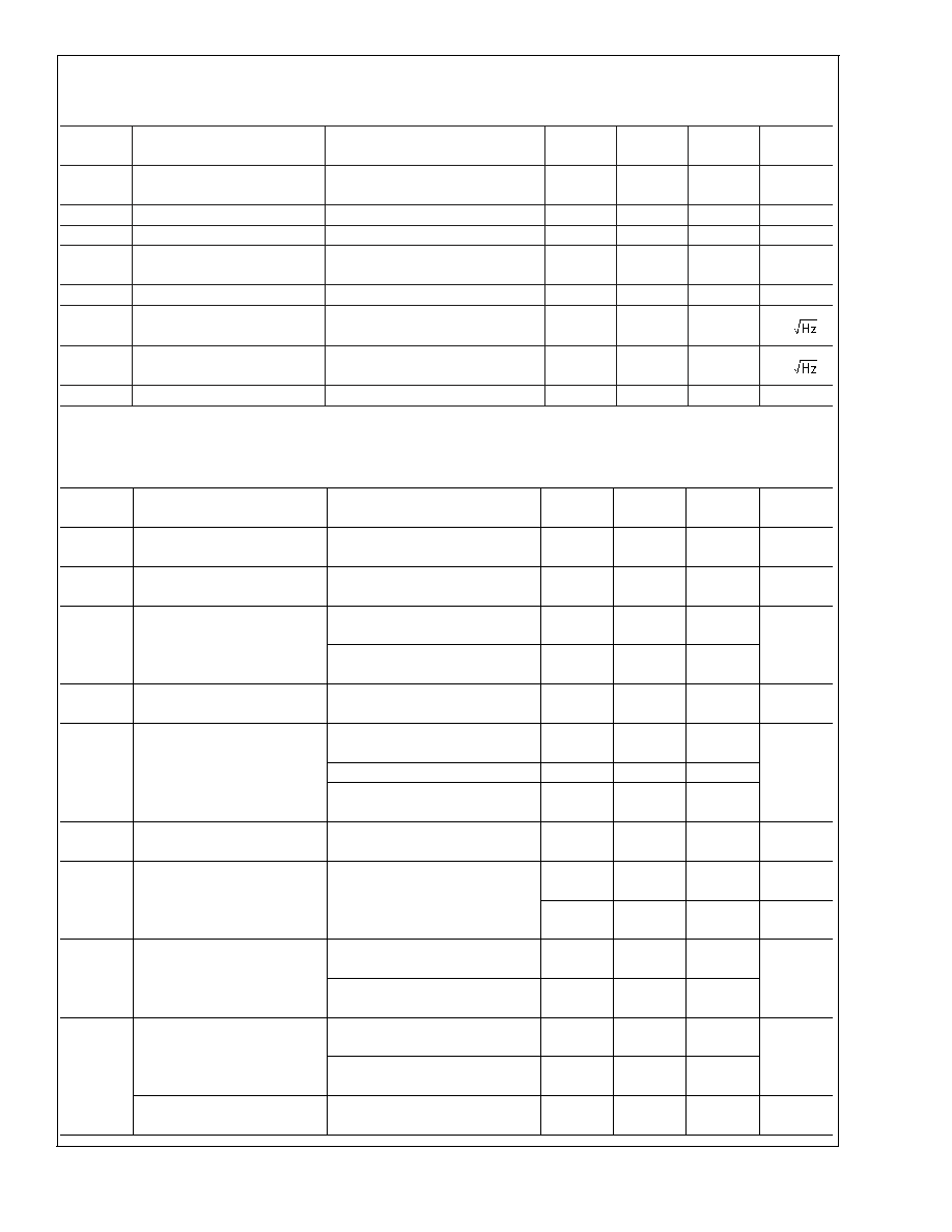
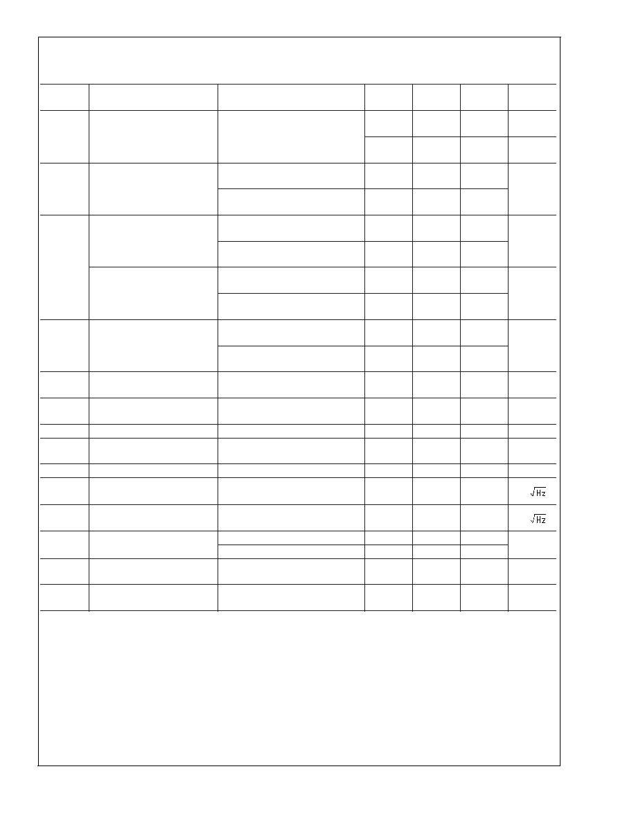
2.7V Electrical Characteristics
Unless otherwise specified, all limits guaranteed for T
J
= 25°C, V
+
= 2.7V, V
-
= 0V, V
CM
= 0.5V, V
O
= V
+
/2, and
R
L
>
1M
to V
-
. Boldface limits apply at the temperature extremes.
Symbol
Parameter
Condition
Min
(Note 6)
Typ
(Note 5)
Max
(Note 6)
Units
V
OS
Input Offset Voltage
V
CM
= 0.5V & V
CM
= 2.2V
+/-0.7
+/-5
+/-7
mV
TC V
OS
Input Offset Average Drift
V
CM
= 0.5V & V
CM
= 2.2V
(Note 12)
+/-2
µV/C
I
B
Input Bias Current
V
CM
= 0.5V
(Note 7)
-1.20
-2.00
-2.70
µA
V
CM
= 2.2V
(Note 7)
+0.49
+1.00
+1.60
I
OS
Input Offset Current
V
CM
= 0.5V & V
CM
= 2.2V
20
250
400
nA
CMRR
Common Mode Rejection
Ratio
V
CM
stepped from 0V to 1.0V
76
60
100
dB
V
CM
stepped from 1.7V to 2.7V
100
V
CM
stepped from 0V to 2.7V
58
50
70
+PSRR
Positive Power Supply
Rejection Ratio
V
+
= 2.7V to 5V
78
74
104
dB
CMVR
Input Common-Mode Voltage
Range
CMRR
>
50dB
-0.3
-0.1
0.0
V
2.8
2.7
3.0
V
A
VOL
Large Signal Voltage Gain
V
O
= 0.5 to 2.2V,
R
L
= 10k to V
-
70
67
78
dB
V
O
= 0.5 to 2.2V,
R
L
= 2k to V
-
67
63
73
dB
V
O
Output Swing
High
R
L
= 10k to V
-
2.49
2.46
2.59
V
R
L
= 2k to V
-
2.45
2.41
2.53
Output Swing
Low
R
L
= 10k to V
-
90
100
120
mV
I
SC
Output Short Circuit Current
Sourcing to V
-
V
ID
= 200mV (Note 10)
30
20
48
mA
Sinking to V
+
V
ID
= -200mV (Note 10)
50
30
65
LM8262
www.national.com
2
2.7V Electrical Characteristics
(Continued)
Unless otherwise specified, all limits guaranteed for T
J
= 25°C, V
+
= 2.7V, V
-
= 0V, V
CM
= 0.5V, V
O
= V
+
/2, and
R
L
>
1M
to V
-
. Boldface limits apply at the temperature extremes.
Symbol
Parameter
Condition
Min
(Note 6)
Typ
(Note 5)
Max
(Note 6)
Units
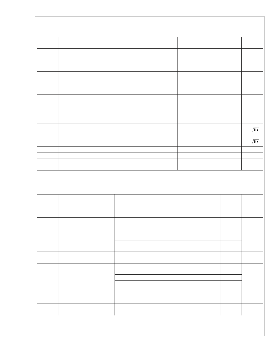
I
S
Supply Current (both amps)
No load, V
CM
= 0.5V
2.0
2.5
3.0
mA
SR
Slew Rate (Note 8)
A
V
= +1,V
I
= 2V
PP
9
V/µs
f
u
Unity Gain-Frequency
V
I
= 10mV, R
L
= 2k
to V
+
/2
10
MHz
GBWP
Gain Bandwidth Product
f = 50KHz
15.5
14
21
MHz
Phi
m
Phase Margin
V
I
= 10mV
50
Deg
e
n
Input-Referred Voltage Noise
f = 2KHz, R
S
= 50
15
nV/
i
n
Input-Referred Current Noise
f = 2KHz
1
pA/
f
max
Full Power Bandwidth
Z
L
= (20pF || 10k
) to V
+
/2
1
MHz
5V Electrical Characteristics
Unless otherwise specified, all limited guaranteed for T
J
= 25°C, V
+
= 5V, V
-
= 0V, V
CM
= 1V, V
O
= V
+
/2, and
R
L
>
1M
to V
-
. Boldface limits apply at the temperature extremes.
Symbol
Parameter
Condition
Min
(Note 6)
Typ
(Note 5)
Max
(Note 6)
Units
V
OS
Input Offset Voltage
V
CM
= 1V & V
CM
= 4.5V
+/-0.7
+/-5
+/- 7
mV
TC V
OS
Input Offset Average Drift
V
CM
= 1V & V
CM
= 4.5V
(Note 12)
+/-2
µV/°C
I
B
Input Bias Current
V
CM
= 1V
(Note 7)
-1.18
-2.00
-2.70
µA
V
CM
= 4.5V
(Note 7)
+0.49
+1.00
+1.60
I
OS
Input Offset Current
V
CM
= 1V & V
CM
= 4.5V
20
250
400
nA
CMRR
Common Mode Rejection
Ratio
V
CM
stepped from 0V to 3.3V
84
72
110
dB
V
CM
stepped from 4V to 5V
100
V
CM
stepped from 0V to 5V
64
61
80
+PSRR
Positive Power Supply
Rejection Ratio
V
+
= 2.7V to 5V, V
CM
= 0.5V
78
74
104
dB
CMVR
Input Common-Mode Voltage
Range
CMRR
>
50dB
-0.3
-0.1
0.0
V
5.1
5.0
5.3
V
A
VOL
Large Signal Voltage Gain
V
O
= 0.5 to 4.5V,
R
L
= 10k to V
-
74
70
84
dB
V
O
= 0.5 to 4.5V,
R
L
= 2k to V
-
70
66
80
V
O
Output Swing
High
R
L
= 10k to V
-
4.75
4.72
4.87
V
R
L
= 2k to V
-
4.70
4.66
4.81
Output Swing
Low
R
L
= 10k to V
-
86
125
135
mV
LM8262
www.national.com
3
5V Electrical Characteristics
(Continued)
Unless otherwise specified, all limited guaranteed for T
J
= 25°C, V
+
= 5V, V
-
= 0V, V
CM
= 1V, V
O
= V
+
/2, and
R
L
>
1M
to V
-
. Boldface limits apply at the temperature extremes.
Symbol
Parameter
Condition
Min
(Note 6)
Typ
(Note 5)
Max
(Note 6)
Units
I
SC
Output Short Circuit Current
Sourcing to V
-
V
ID
= 200mV (Note 10)
35
20
53
mA
Sinking to V
+
V
ID
= -200mV (Note 10)
60
50
75
I
S
Supply Current (both amps)
No load, V
CM
= 1V
2.3
2.8
3.5
mA
SR
Slew Rate (Note 8)
A
V
= +1, V
I
= 5V
PP
10
7
12
V/µs
f
u
Unity Gain Frequency
V
I
= 10mV,
R
L
= 2k
to V
+
/2
10.5
MHz
GBWP
Gain-Bandwidth Product
f = 50KHz
16
15
21
MHz
Phi
m
Phase Margin
V
I
= 10mV
53
Deg
e
n
Input-Referred Voltage Noise
f = 2KHz, R
S
= 50
15
nV/
i
n
Input-Referred Current Noise
f = 2KHz
1
pA/
f
max
Full Power Bandwidth
Z
L
= (20pF || 10k
) to V
+
/2
900
KHz
t
S
Settling Time (+/-5%)
100mV
PP
Step, 500pF load
400
ns
THD+N
Total Harmonic Distortion +
Noise
R
L
= 1k
to V
+
/2
f = 10KHz to A
V
= +2, 4V
PP
swing
0.05
%
+/-11V Electrical Characteristics
Unless otherwise specified, all limited guaranteed for T
J
= 25°C, V
+
= 11V, V
-
= -11V, V
CM
= 0V, V
O
= 0V, and
R
L
>
1M
to 0V. Boldface limits apply at the temperature extremes.
Symbol
Parameter
Condition
Min
(Note 6)
Typ
(Note 5)
Max
(Note 6)
Units
V
OS
Input Offset Voltage
V
CM
= -10.5V & V
CM
= 10.5V
+/-0.7
+/-7
+/- 9
mV
TC V
OS
Input Offset Average Drift
V
CM
= -10.5V & V
CM
= 10.5V
(Note 12)
+/-2
µV/°C
I
B
Input Bias Current
V
CM
= -10.5V
(Note 7)
-1.05
-2.00
-2.80
µA
V
CM
= 10.5V
(Note 7)
+0.49
+1.00
+1.50
I
OS
Input Offset Current
V
CM
= -10.5V & V
CM
= 10.5V
30
275
550
nA
CMRR
Common Mode Rejection
Ratio
V
CM
stepped from -11V to 9V
84
80
100
dB
V
CM
stepped from 10V to 11V
100
V
CM
stepped from -11V to 11V
74
72
88
+PSRR
Positive Power Supply
Rejection Ratio
V
+
= 9V to 11V
70
66
100
dB
-PSRR
Negative Power Supply
Rejection Ratio
V
-
= -9V to -11V
70
66
100
dB
LM8262
www.national.com
4
+/-11V Electrical Characteristics
(Continued)
Unless otherwise specified, all limited guaranteed for T
J
= 25°C, V
+
= 11V, V
-
= -11V, V
CM
= 0V, V
O
= 0V, and
R
L
>
1M
to 0V. Boldface limits apply at the temperature extremes.
Symbol
Parameter
Condition
Min
(Note 6)
Typ
(Note 5)
Max
(Note 6)
Units
CMVR
Input Common-Mode Voltage
Range
CMRR
>
50dB
-11.3
-11.1
-11.0
V
11.1
11.0
11.3
V
A
VOL
Large Signal Voltage Gain
V
O
= 0V to +/-9V,
R
L
= 10k
78
74
85
dB
V
O
= 0V to +/-9V,
R
L
= 2k
72
66
79
V
O
Output Swing
High
R
L
= 10k
10.65
10.61
10.77
V
R
L
= 2k
10.6
10.55
10.69
Output Swing
Low
R
L
= 10k
-10.98
-10.75
-10.65
V
R
L
= 2k
-10.91
-10.65
-10.6
I
SC
Output Short Circuit Current
Sourcing to ground
V
ID
= 200mV (Note 10)
40
25
60
mA
Sinking to ground
V
ID
= 200mV (Note 10)
65
55
100
I
S
Supply Current
No load, V
CM
= 0V
2.5
4
5
mA
SR
Slew Rate
(Note 8)
A
V
= +1, V
I
= 16V
PP
10
8
15
V/µs
f
U
Unity Gain Frequency
V
I
= 10mV, R
L
= 2k
13
MHz
GBWP
Gain-Bandwidth Product
f = 50KHz
18
16
24
MHz
Phi
m
Phase Margin
V
I
= 10mV
58
Deg
e
n
Input-Referred Voltage Noise
f = 2KHz, R
S
= 50
15
nV/
i
n
Input-Referred Current Noise
f = 2KHz
1
pA/
t
S
Settling Time (+/-1%, A
V
=
+1)
Positive Step, 5V
PP
320
ns
Negative Step, 5V
PP
600
THD+N
Total Harmonic Distortion
+Noise
R
L
= 1k
, f = 10KHz,
A
V
= +2, 15V
PP
swing
0.01
%
CT
REJ
Cross-Talk Rejection
f = 5MHz, Driver
R
L
= 10k
68
dB
LM8262
www.national.com
5
Document Outline