 | –≠–ª–µ–∫—Ç—Ä–æ–Ω–Ω—ã–π –∫–æ–º–ø–æ–Ω–µ–Ω—Ç: LM831N | –°–∫–∞—á–∞—Ç—å:  PDF PDF  ZIP ZIP |
TL H 6754
LM831
Low
Voltage
Audio
Power
Amplifier
December 1994
LM831 Low Voltage Audio Power Amplifier
General Description
The LM831 is a dual audio power amplifier optimized for
very low voltage operation The LM831 has two indepen-
dent amplifiers giving stereo or higher power bridge (BTL)
operation from two- or three-cell power supplies
The LM831 uses a patented compensation technique to re-
duce high-frequency radiation for optimum performance in
AM radio applications This compensation also results in
lower distortion and less wide-band noise
The input is direct-coupled to the LM831 eliminating the
usual coupling capacitor Voltage gain is adjustable with a
single resistor
Features
Y
Low voltage operation 1 8V to 6 0V
Y
High power 440 mW 8X BTL 3V
Y
Low AM radiation
Y
Low noise
Y
Low THD
Applications
Y
Portable tape recorders
Y
Portable radios
Y
Headphone stereo
Y
Portable speakers
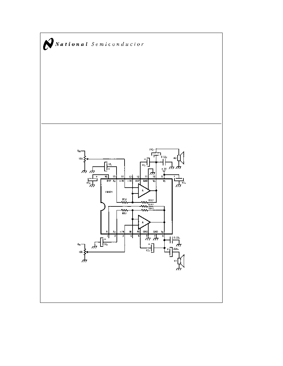
Typical Application
Dual Amplifier with Minimum Parts
TL H 6754 ≠ 1
A
V
e
46 dB BW
e
250 Hz to 35 kHz
P
OUT
e
220 mW Ch R
L
e
4X
C1995 National Semiconductor Corporation
RRD-B30M115 Printed in U S A

Absolute Maximum Ratings
If Military Aerospace specified devices are required
please contact the National Semiconductor Sales
Office Distributors for availability and specifications
Supply Voltage V
S
7 5V
Input Voltage V
IN
g
0 4V
Power Dissipation (Note 1) P
D
1 3W (M Package)
1 4W (N Package)
Operating Temperature (Note 1) T
opr
b
40 C to
a
85 C
Storage Temperature T
stg
b
65 C to
a
150 C
Junction Temperature T
j
a
150 C
Lead Temp (Soldering 10 sec ) T
L
a
260 C
Thermal Resistance
i
JC
(DIP)
27 C W
i
JA
(DIP)
75 C W
i
JC
(SO Package)
20 C W
i
JA
(SO Package)
95 C W
Electrical Characteristics
Unless otherwise specified T
A
e
25 C V
S
e
3V f
e
1 kHz test circuit is dual or BTL amplifier with minimum parts
Symbol
Parameter
Conditions
Typ
Tested Limit
Unit (Limit)
V
S
Operating Voltage
3
1 8
V(Min)
3
6
V(Max)
I
Q
Supply Current
V
IN
e
0 Dual Mode
5
10
mA (Max)
V
IN
e
0 BTL Mode
6
15
mA (Max)
V
OS
Output DC Offset
V
IN
e
0 BTL Mode
10
50
mV (Max)
R
IN
Input Resistance
25
15
k (Min)
35
k (Max)
A
V
Voltage Gain
V
IN
e
2 25 mV
rms
f
e
1 kHz
46
44
dB (Min)
Dual Mode
48
dB (Max)
PSRR
Supply Rejection
V
S
e
3V
a
200 mV
rms
f
e
1 kHz
46
30
dB (Min)
P
OD
Power Out
V
S
e
3V R
L
e
4X
220
150
mW (Min)
10% THD Dual Mode
P
ODL
Power Out Low V
S
V
S
e
1 8V R
L
e
4X
45
10
mW (Min)
10% THD Dual Mode
P
OB
Power Out
V
S
e
3V R
L
e
8X
440
300
mW (Min)
10% THD BTL Mode
P
OBL
Power Out Low V
S
V
S
e
1 8V R
L
e
8X
90
20
mW (Min)
10% THD BTL Mode
Sep
Channel Separation
Referenced to V
O
e
200 mV
rms
52
40
dB (Min)
I
B
Input Bias Current
1
2
m
A (Max)
E
n0
Output Noise
Wide Band (250 E 35 kHz)
250
500
m
V (Max)
THD
Distortion
V
S
e
3V P
O
e
50 mW
0 25
1
% (Max)
f
e
1 kHz Dual
Note 1
For operation in ambient temperatures above 25 C the device must be derated based on a 150 C maximum junction temperature and a thermal resistance
of 98 C W junction to ambient for the M package or 90 C W junction to ambient for the N package
Connection Diagram
Dual-In-Line Package
TL H 6754 ≠ 2
Top View
Order Number LM831M or N
See NS Package Number M16B or N16E
2

Typical Performance Characteristics
Supply Current vs Supply Voltage
PSRR vs Supply Voltage
Supply Current vs Temperature
PSRR vs Supply Voltage
DC Output vs Supply Voltage
Separation vs Supply Voltage
TL H 6754 ≠ 4
3
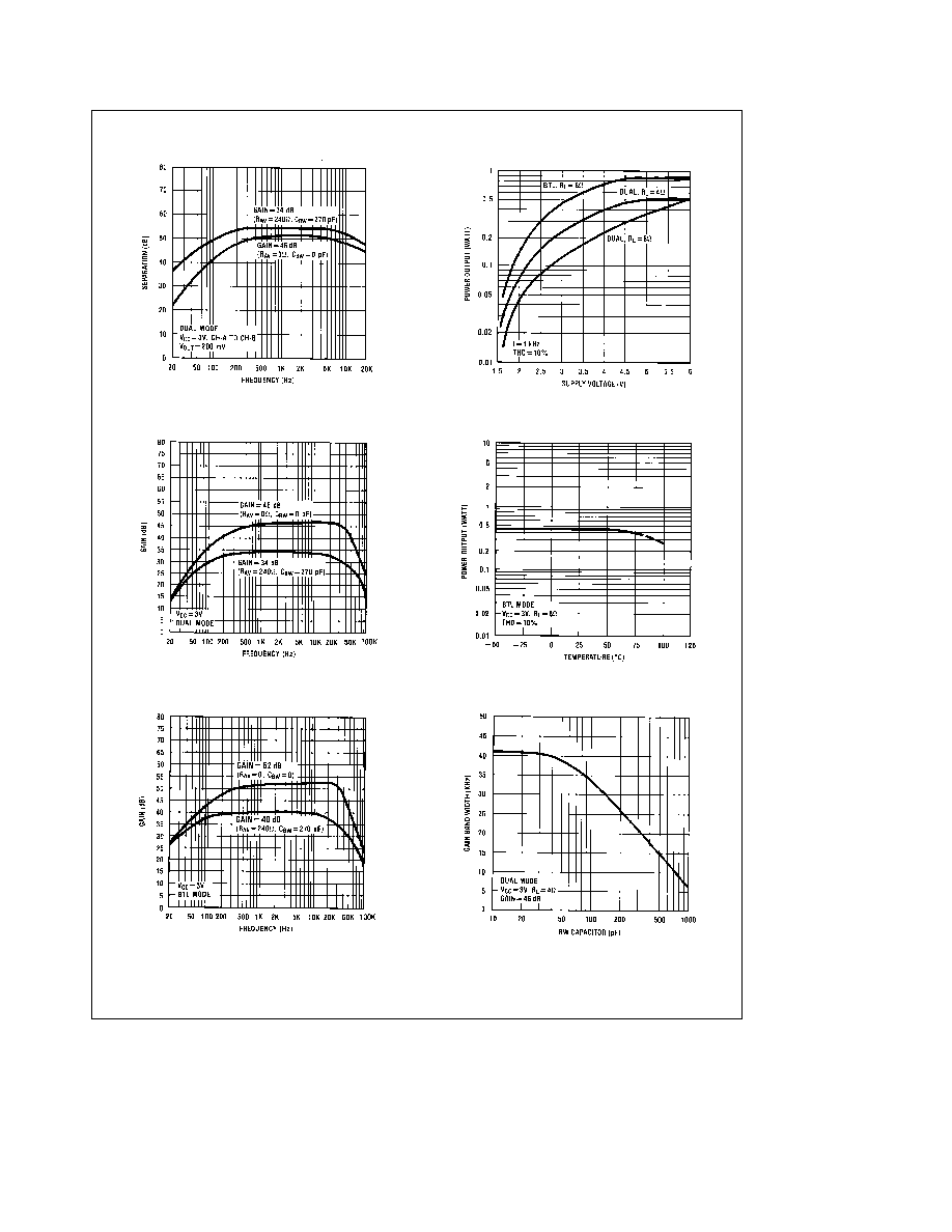
Typical Performance Characteristics
(Continued)
Separation vs Frequency
Power Output vs Supply Voltage
Gain vs Frequency
Power Output vs Temperature
Gain vs Frequency
Bandwidth vs BW Capacitance
TL H 6754 ≠ 5
4

Typical Performance Characteristics
(Continued)
Dual Mode R
L
e
4X Distortion vs Frequency
Dual Mode R
L
e
8X Distortion vs Frequency
Distortion vs Power Output
(Note 2)
Distortion vs Power Output
(Note 2)
Power Dissipation vs Power Output
Power Dissipation vs Power Output
TL H 6754 ≠ 6
5