LM8364
Micropower Undervoltage Sensing Circuits
General Description
The LM8364 series are micropower undervoltage sensing
circuits that are ideal for use in battery powered micropro-
cessor based systems, where extended battery life is a key
requirement.
A range of threshold voltages from 2.0V to 4.5V are available
with an active low open drain output. These devices feature
a very low quiescent current of 0.65µA typical. The LM8364
series features a highly accurate voltage reference, a com-
parator with precise thresholds and built-in hysterisis to pre-
vent erratic reset operation, and guaranteed Reset operation
down to 1.0V with extremely low standby current.
These devices are available in the space saving SOT23
5-pin surface mount package. For other undervoltage
thresholds and output options, please contact National
Semiconductor.
Features
n
Extremely Low Quiescent Current: 0.65µA, at V
IN
=
2.87V
n
High Accuracy Threshold Voltage (
±
2.5%)
n
Open Drain Output
n
Input Voltage Range: 1V to 6V
n
Surface Mount Package (5-Pin SOT23)
n
Pin for pin compatible with MC33464
Applications
n
Low Battery Detection
n
Microprocessor reset Controller
n
Power Fail Indicator
n
Battery Backup Detection
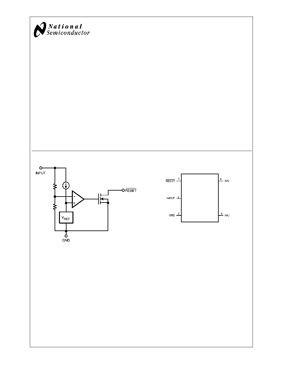
Functional Block Diagram
20065907
Connection Diagram
5-Pin SOT23
20065906
Top View
March 2003
LM8364
Micropower
Undervoltage
Sensing
Circuits
© 2003 National Semiconductor Corporation
DS200659
www.national.com

Pin Description
20065908
Ordering Information
Package
Part Number
Package
Marking
Threshold
Output Type
Transport Media
NSC Drawing
5-Pin
SOT23
LM8364BALMF20
F01A
2.0V
Open Drain,
Active Low
1k Units Tape and Reel
MF05A
LM8364BALMFX20
3k Units Tape and Reel
LM8364BALMF30
F05A
3.0V
Open Drain,
Active Low
1k Units Tape and Reel
LM8364BALMFX30
3k Units Tape and Reel
LM8364BALMF45
F04A
4.5V
Open Drain,
Active Low
1k Units Tape and Reel
LM8364BALMFX45
3k Units Tape and Reel
LM8364
www.national.com
2

Absolute Maximum Ratings
(Note 1)
If Military/Aerospace specified devices are required,
please contact the National Semiconductor Sales Office/
Distributors for availability and specifications.
Supply Voltage
-0.3V to 6.5V
RESET Output Voltage
-0.3V to 6.5V
RESET Output Current
70mA
Storage Temperature Range
-65∞C to 150∞C
Mounting Temp.
Lead temp (Soldering, 10 sec)
260∞C
Junction Temperature
125∞
Operating Ratings
(Note 1)
Temperature Range
-40∞C to 85∞C
Thermal Resistance to ambient (
JA
)
265∞C/W
ESD Tolerance
Human Body Model
2000V
Machine Model
200V
Electrical Characteristics
Unless otherwise specified, all limits guaranteed for T
A
= 25∞C.
Symbol
Parameter
Conditions
Min
(Note 3)
Typ
(Note 2)
Max
(Note 3)
Units
V
DET-
Detector Threshold Voltage
High to Low State Output
(V
IN
Decreasing)
V
20 Suffix
1.950
2.0
2.050
30 Suffix
2.925
3.0
3.075
45 Suffix
4.388
4.5
4.613
V
HYS
Detector Threshold
Hysteresis
V
IN
Increasing
V
20 Suffix
0.060
0.100
0.140
30 Suffix
0.090
0.150
0.210
45 Suffix
0.135
0.225
0.315
Vdet/T
Detector Threshold Voltage
Temperature Coefficient
±
100
PPM/∞C
V
OL
RESET Output Voltage Low
State
(Open Drain Output: I
SINK
= 1mA)
0.25
0.5
V
I
OL
RESET Output Sink Current
V
IN
= 1.5V, V
OL
= 0.5V
1.0
2.5
mA
V
IN
Operating Input Voltage
Range
1.0
6.0
V
I
IN
Quiescent Input Current
20 Suffix
µA
V
IN
= 1.9V
0.55
0.8
V
IN
= 4.0V
0.70
1.3
30 Suffix
V
IN
= 2.87V
0.65
0.9
V
IN
= 5.0V
0.77
1.3
45 Suffix
V
IN
= 4.34V
0.70
1.0
V
IN
= 6.0
0.85
1.4
t
p
Propagation Delay Time
Figure 1
60
300
µs
Note 1: Absolute Maximum Ratings indicate limits beyond which damage to the device may occur. Operating Ratings indicate conditions for which the device is
intended to be functional, but specific performance is not guaranteed. For guaranteed specifications and the test conditions, see the Electrical Characteristics.
Note 2: Typical values represent the most likely parametric norm
Note 3: All limits are guaranteed by testing or statistical analysis.
LM8364
www.national.com
3

Typical Performance Characteristics
Input Current vs. Input Voltage
LM8364BALMF45
Reset Output Voltage vs. Input Voltage
LM8364BALMF45
20065901
20065902
Reset Output Sink Current vs. Input Voltage
LM8364BALMF45
Reset Output Sink Current vs. Output Voltage
LM8364BALMF45
20065903
20065904
Detector Threshold Voltage vs. Temperature
LM8364BALMF45
20065905
LM8364
www.national.com
4

Application Notes
The propagation delay time for the LM8364 is measured
using a 470k
pull-up resistor connected to from the RESET
output pin to 5V in addition to a 10pF capacitive load con-
nected from the same pin to GND. Figure 1 shows the timing
diagram for the measurement for the propagation delay.
V
DET+
is equal to the sum of the detector threshold, V
DET-
,
and the built in hysteresis, V
HYS
.
The LM8364 ultra-low current voltage detector was designed
to monitor voltages and to provide an indication when the
monitored voltage, V
IN
, dropped below a precisely trimmed
threshold voltage. This characteristic is displayed in the typi-
cal operating timing diagram below. V
IN
is the voltage that is
being monitored and a pull up resistor is connected from the
RESET output pin to V
IN
. V
IN
is at some value above V
DET+
and then begins to decrease. Since this is an Active Low
device the RESET output is pulled High through the pull-up
resistor and tracks V
IN
until V
IN
crosses the trimmed thresh-
old V
DET-
. At this point the LM8364 recognizes that V
IN
is
now in a fault condition and the output immediately changes
to the Logic Low State. The RESET output will remain in this
low state until V
IN
increases above the threshold V
DET-
+
V
HYS
. This point is also known as V
DET+
as indicated earlier.
This built-in hysteresis has been added to the design to help
prevent erratic reset operation when the input voltage
crosses the threshold.
The LM8364 has a wide variety of applications that can take
advantage of its precision and low current consumption to
monitor Input voltages even though it was designed as a
reset controller in portable microprocessor based systems. It
is a very cost effective and space saving device that will
protect your more expensive investments of microproces-
sors and other devices that need a guaranteed supply volt-
age for proper operation.
20065909
FIGURE 1. Propagation Delay Timing Diagrams
20065910
FIGURE 2. Timing Waveforms
LM8364
www.national.com
5