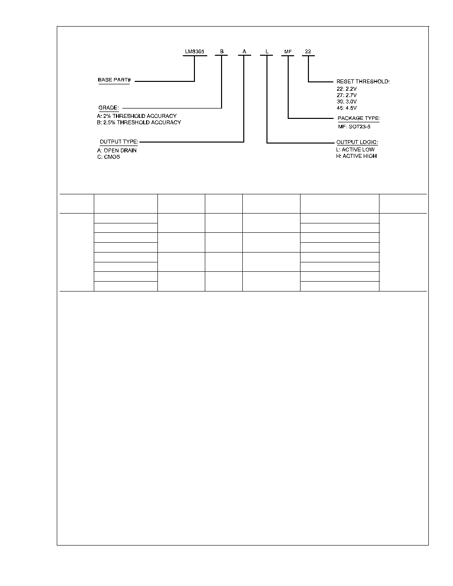
LM8365
Micropower Undervoltage Sensing Circuits with
Programmable Output Delay
General Description
The LM8365 series are micropower undervoltage sensing
circuits that are ideal for use in battery powered micropro-
cessor based systems, where extended battery life is a key
requirement.
A range of threshold voltages from 2.0V to 4.5V are available
with an active low, open drain or CMOS, output. These
devices feature a very low quiescent current of 0.65µA typi-
cal. The LM8365 series features a highly accurate voltage
reference, a comparator with precise thresholds and built-in
hysterisis to prevent erratic reset operation, a time delayed
output which can be programmed by the system designer,
and guaranteed Reset operation down to 1.0V with ex-
tremely low standby current.
These devices are available in the space saving 5-Pin
SOT23 surface mount package. For additional undervoltage
thresholds and output options, please contact National
Semiconductor.
Features
n
Extremely Low Quiescent Current: 0.65µA, at V
IN
=
2.87V
n
High Accuracy Threshold Voltage (
±
2.5%)
n
Complementary or Open Drain Output
n
Programmable output delay by external Capacitor
(100ms typ with 0.1µF)
n
Input Voltage Range: 1V to 6V
n
Surface Mount Package (5-Pin SOT23)
n
Pin for pin compatible with MC33465
Applications
n
Low Battery Detection
n
Microprocessor Reset Controller
n
Power Fail Indicator
n
Battery Backup Detection
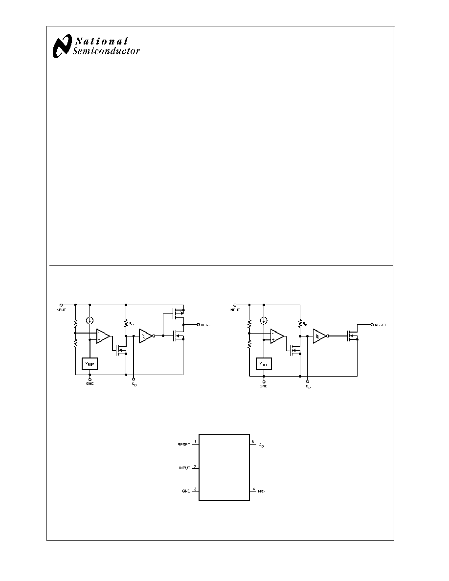
Functional Diagrams
CMOS Output
Open Drain Output
20066013
20066014
Connection Diagram
5-Pin SOT23
20066012
Top View
March 2003
LM8365
Micropower
Undervoltage
Sensing
Circuits
with
Programmable
Output
Delay
© 2003 National Semiconductor Corporation
DS200660
www.national.com
Pin Description
20066015
Ordering Information
Package
Part Number
Package
Marking
Threshold
Output Type
Transport Media
NSC Drawing
5-Pin
SOT23
LM8365BALMF22
F08A
2.2V
Open Drain,
Active Low
1k Units Tape and Reel
MF05A
LM8365BALMFX22
3k Units Tape and Reel
LM8365BALMF27
F07A
2.7V
Open Drain,
Active Low
1k Units Tape and Reel
LM8365BALMFX27
3k Units Tape and Reel
LM8365BCLMF30
F02A
3.0V
CMOS, Active
Low
1k Units Tape and Reel
LM8365BCLMFX30
3k Units Tape and Reel
LM8365BALMF45
F06A
4.5V
Open Drain,
Active Low
1k Units Tape and Reel
LM8365BALMFX45
3k Units Tape and Reel
LM8365
www.national.com
2
Absolute Maximum Ratings
(Note 1)
If Military/Aerospace specified devices are required,
please contact the National Semiconductor Sales Office/
Distributors for availability and specifications.
Supply Voltage
-0.3V to 6.5V
RESET Output Voltage
-0.3V to 6.5V
RESET Output Current
70mA
Storage Temperature Range
-65∞C to 150∞C
Mounting Temperature
Lead Temp. (Soldering 10 sec)
260∞C
Junction Temperature
125∞C
Operating Ratings
(Note 1)
Temperature Range
-40∞C to 85∞C
Thermal Resistance to Ambient (
JA
)
265∞C/W
ESD Tolerance
Human Body Model
2000V
Machine Model
200V
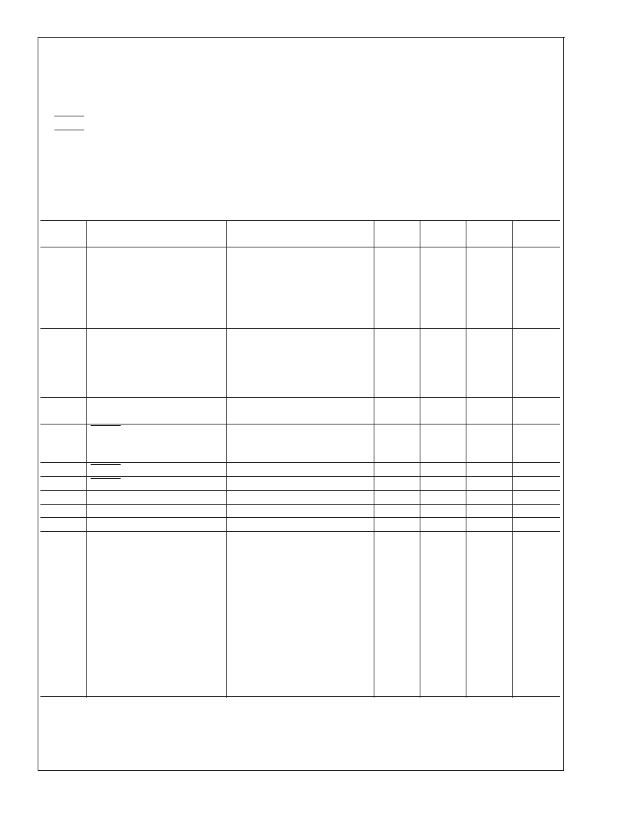
Electrical Characteristics
Unless otherwise specified, all limits guaranteed for T
A
= 25∞C.
Symbol
Parameter
Conditions
Min
(Note 3)
Typ
(Note 2)
Max
(Note 3)
Units
V
DET-
Detector Threshold Voltage
High to Low State Output
(V
IN
Decreasing)
V
22 Suffix
2.145
2.2
2.255
27 Suffix
2.633
2.7
2.767
30 Suffix
2.925
3.0
3.075
45 Suffix
4.388
4.5
4.613
V
HYS
Detector Threshold Hysteresis
V
IN
Increasing
V
22 Suffix
0.066
0.110
0.154
27 Suffix
0.081
0.135
0.189
30 Suffix
0.090
0.150
0.210
45 Suffix
0.135
0.225
0.315
Vdet/T Detector Threshold Voltage
Temperature Coefficient
±
100
PPM/∞C
V
OH
V
OL
RESET Output Voltage
(CMOS Output: I
SOURCE
= 1mA)
(Open Drain or CMOS Output:
I
SINK
= 1mA)
V
IN
-2.1
V
IN
-1.0
0.25
V
IN
0.5
V
I
OL
RESET Output Sink Current
V
IN
= 1.5V, V
OL
= 0.5V
1.0
2.5
mA
I
OH
RESET Output Source Current
V
IN
= 4.5V, V
OL
= 2.4V
1.0
7.0
mA
I
CD
Delay Pin Output Sink Current
V
IN
= 1.5V, V
CD
= 0.5V
0.2
1.8
mA
R
D
Delay Resistance
0.5
1.0
2.0
M
V
IN
Operating Input Voltage Range
1.0
6.0
V
I
IN
Quiescent Input Current
22 Suffix
µA
V
IN
= 2.10V
0.57
0.8
V
IN
= 4.20V
0.71
1.3
27 Suffix
V
IN
= 2.60V
0.62
0.9
V
IN
= 4.70V
0.75
1.3
30 Suffix
V
IN
= 2.87V
0.65
0.9
V
IN
= 5.00V
0.77
1.3
45 Suffix
V
IN
= 4.34V
0.70
1.0
V
IN
= 6.00V
0.85
1.4
Note 1: Absolute Maximum Ratings indicate limits beyond which damage to the device may occur. Operating Ratings indicate conditions for which the device is
intended to be functional, but specific performance is not guaranteed. For guaranteed specifications and the test conditions, see the Electrical Characteristics.
Note 2: Typical values represent the most likely parametric norm.
Note 3: All limits are guaranteed by testing or statistical analysis.
LM8365
www.national.com
3
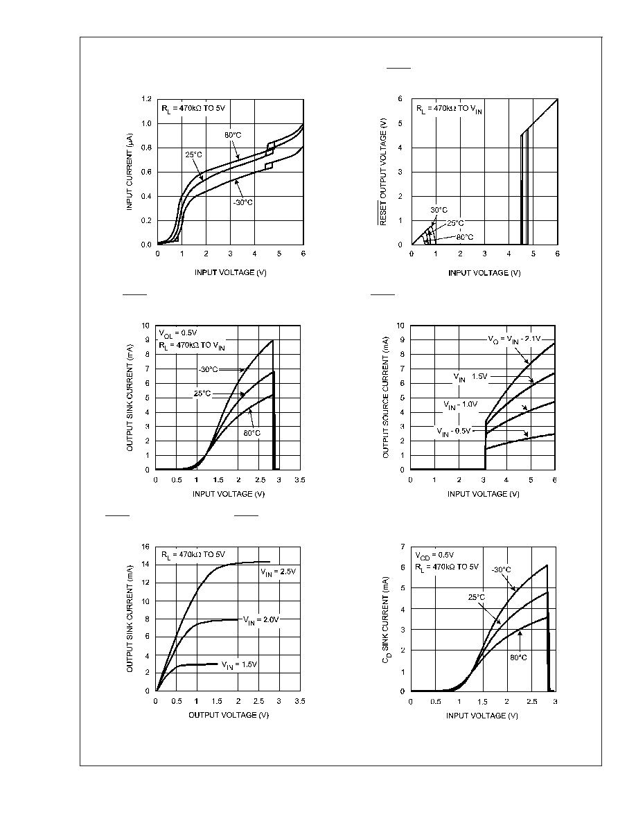
Typical Performance Characteristics
Input Current vs. Input Voltage
LM8365BALMF45
Reset Output Voltage vs. Input Voltage
LM8365BALMF45
20066001
20066002
Reset Output Sink Current vs. Input Voltage
LM8365BALMF27
Reset Output Source Current vs. Input Voltage
LM8365BCLMF30
20066003
20066004
Reset Output Sink Current vs. Reset Output Voltage
LM8365BALMF45
C
D
Sink Current vs. Input Voltage
LM8365BALMF27
20066005
20066006
LM8365
www.national.com
4

Typical Performance Characteristics
(Continued)
C
D
Sink Current vs. C
D
Voltage
C
D
Delay Pin Threshold Voltage vs. Temperature
LM8365BALMF27
20066007
20066008
Detector Threshold Voltage vs. Temperature
LM8365BALMF45
Delay Resistance vs. Temperature
20066009
20066010
Output Time Delay vs. Capacitance
20066011
LM8365
www.national.com
5