 | –≠–ª–µ–∫—Ç—Ä–æ–Ω–Ω—ã–π –∫–æ–º–ø–æ–Ω–µ–Ω—Ç: LM87CIMT | –°–∫–∞—á–∞—Ç—å:  PDF PDF  ZIP ZIP |

LM87
Serial Interface System Hardware Monitor with Remote
Diode Temperature Sensing
General Description
The LM87 is a highly integrated data acquisition system for
hardware monitoring of servers, Personal Computers, or
virtually any microprocessor-based system. In a PC, the
LM87 can be used to monitor power supply voltages, moth-
erboard and processor temperatures, and fan speeds. Ac-
tual values for these inputs can be read at any time. Pro-
grammable WATCHDOG limits in the LM87 activate a fully
programmable and maskable interrupt system with two out-
puts (INT# and THERM#).
The LM87 has an on-chip digital output temperature sensor
with 8-bit resolution as well as the capability of monitoring 2
external diode temperatures to 8-bit resolution, an 8 channel
analog input ADC with 8-bit resolution and an 8-bit DAC. A
channel on the ADC measures the supply voltage applied to
the LM87, nominally 3.3 V. Two of the ADC inputs can be
redirected to a counter that can measure the speed of up to
2 fans. A slow speed
ADC architecture allows stable
measurement of signals in an extremely noisy environment.
The DAC, with a 0 to 2.5 V output voltage range, can be
used for fan speed control. Additional inputs are provided for
Chassis Intrusion detection circuits, and VID monitor inputs.
The VID monitor inputs can also be used as IRQ inputs if VID
monitoring is not required. The LM87 has a Serial Bus
interface that is compatible with SMBus
TM
and I
2
C
TM
.
Features
n
Remote diode temperature sensing (2 channels)
n
8 positive voltage inputs with scaling resistors for
monitoring +5 V, +12 V, +3.3 V, +2.5 V, Vccp power
supplies directly
n
2 inputs selectable for fan speed or voltage monitoring
n
8-bit DAC output for controlling fan speed
n
Chassis Intrusion Detector input
n
WATCHDOG comparison of all monitored values
n
SMBus or I
2
C Serial Bus interface compatibility
n
VID0-VID4 or IRQ0-IRQ4 monitoring inputs
n
On chip temperature sensor
Key Specifications
j
Voltage Monitoring Error
±
2 % (max)
j
External Temperature Error
±
4 ∞C (max)
j
Internal Temperature Error
-40 ∞C to +125 ∞C
±
3 ∞C (typ)
j
Supply Voltage Range
2.8 to 3.8 V
j
Supply Current
0.7 mA (typ)
j
ADC and DAC Resolution
8 Bits
j
Temperature Resolution
1.0 ∞C
Applications
n
System Thermal and Hardware Monitoring for Servers,
Workstations and PCs
n
Networking and Telecom Equipment
n
Office Electronics
n
Electronic Test Equipment and Instrumentation
Ordering Information
Temperature Range
NS Package
Number
-40 ∞C
T
A
+125 ∞C
Order Number
Device Marking
LM87CIMT
1
LM87CIMT
MTC24B
LM87CIMTX
2
LM87CIMT
MTC24B
Note:
1
-Rail transport media, 61 parts per rail
2
-Tape and reel transport media, 2500 parts per reel
Connection Diagram
10099503
SMBus
TM
is a trademark of the Intel Corporation.
December 2003
LM87
Serial
Interface
System
Hardware
Monitor
with
Remote
Diode
T
emperature
Sensing
© 2003 National Semiconductor Corporation
DS100995
www.national.com

Block Diagram
10099501
Pin Description
Pin
Name(s)
Pin
Number
Number
of Pins
Type
Description
ADD/NTEST_OUT
1
1
Digital I/0
This pin normally functions as a three-state input that controls the
two LSBs of the Serial Bus Address. When this pin is tied to V
CC
the two LSBs are 01. When tied to Ground, the two LSBs are 10. If
this pin is not connected, the two LSBs are 00. This pin also
functions as an output during NAND Tree tests (board-level
connectivity testing). To ensure proper NAND tree function, this pin
should not be tied directly to V
CC
or Ground. Instead, a series 5 k
resistor should be used to allow the test output function to work.
Refer to SECTION 11 on NAND Tree testing.
THERM#
2
1
Digital I/O
This pin functions as an open-drain interrupt output for temperature
interrupts only, or as an interrupt input for fan control. It has an
on-chip 100 k
pullup resistor.
SMBData
3
1
Digital I/O
Serial Bus bidirectional Data. Open-drain output.
SMBCLK
4
1
Digital Input
Serial Bus Clock.
FAN1/AIN1-
FAN2/AIN2
5-6
2
Analog/Digital
Inputs
Programmable as analog inputs (0 to 2.5V) or digital Schmitt
Trigger fan tachometer inputs.
CI
7
1
Digital I/O
An active high input from an external circuit which latches a
Chassis Intrusion event. This line can go high without any clamping
action regardless of the powered state of the LM87. There is also
an internal open-drain output on this line, controlled by Bit 7 of the
CI Clear Register (46h), to provide a minimum 20 ms pulse.
LM87
www.national.com
2

Pin Description
(Continued)
Pin
Name(s)
Pin
Number
Number
of Pins
Type
Description
GND
8
1
GROUND
The system ground pin. Internally connected to all circuitry. The
ground reference for all analog inputs and the DAC output. This pin
needs to be connected to a low noise analog ground plane for
optimum performance of the DAC output.
V
+
(+2.8 V to
+3.8 V)
9
1
POWER
+3.3 V V
+
power. Bypass with the parallel combination of 10 µF
(electrolytic or tantalum) and 0.1 µF (ceramic) bypass capacitors.
INT# /ALERT#
10
1
Digital Output
Interrupt active low open-drain output. This output is enabled when
Bit 1 in the Configuration Register is set to 1. The default state is
disabled. It has an on-chip 100 k
pullup resistor. Alternately used
as an active low output to signal SMBus Alert Response Protocol.
DACOut/NTEST_IN
11
1
Analog
Output/Digital
Input
0 V to +2.5 V amplitude 8-bit DAC output. When forced high on
power up by an external voltage the NAND Tree Test mode is
enabled which provides board-level connectivity testing.
RESET#
12
1
Digital I/O
Master Reset, 5 mA driver (open-drain), active low output with a 20
ms minimum pulse width. Available when enabled via Bit 4 in the
Configuration register. It also acts as an active low power on
RESET input. It has an on-chip 100 k
pullup resistor.
D1-
13
1
Analog Input
Analog input for monitoring the cathode of the first external
temperature sensing diode.
D1+
14
1
Analog Input
Analog input for monitoring the anode of the first external
temperature sensing diode.
+12Vin
15
1
Analog Input
Analog input for monitoring +12 V.
+5Vin
16
1
Analog Input
Analog input for monitoring +5 V.
Vccp2/D2-
17
1
Analog Input
Digitally programmable analog input for monitoring Vccp2 (0 to 3.6
V input range) or the cathode of the second external temperature
sensing diode.
+2.5Vin/D2+
18
1
Analog Input
Digitally programmable analog input for monitoring +2.5 V or the
anode of the second external temperature sensing diode.
Vccp1
19
1
Analog Input
Analog input (0 to 3.6 V input range) for monitoring Vccp1, the core
voltage of processore 1.
VID4/IRQ4-
VID0/IRQ0
20-24
5
Digital Inputs
Digitally programmable dual function digital inputs. Can be
programmed to monitor the VID pins of the Pentium/PRO and
Pentium II processors, that indicate the operating voltage of the
processor, or as interrupt inputs. The values are read in the
VID/Fan Divisor Register and the VID4 Register. These inputs have
on-chip 100 k
pullup resistors.
TOTAL PINS
24
# Indicates Active Low ("Not")
LM87
www.national.com
3
Absolute Maximum Ratings
(Notes 1,
2)
If Military/Aerospace specified devices are required,
please contact the National Semiconductor Sales Office/
Distributors for availability and specifications.
Positive Supply Voltage (V
+
)
+6.0 V
Voltage on Any Input or Output Pin:
+12Vin
-0.3 V to +18 V
ADD/NTESTOUT,
DACOut/NTEST_IN, AIN1, AIN2
-0.3 V to
(V
+
+ 0.3 V)
All other pins
-0.3 V to +6 V
Input Current at any Pin (Note 4)
±
5 mA
Package Input Current (Note 4)
±
20 mA
Maximum Junction Temperature
(T
J
max)
150 ∞C
ESD Susceptibility (Note 6)
Human Body Model
2500 V
Machine Model
150V
Soldering Information
MTC Package (Note 7) :
Vapor Phase (60 seconds)
215 ∞C
Infrared (15 seconds)
235 ∞C
Storage Temperature
-65 ∞C to +150 ∞C
Operating Ratings
(Notes 1, 2)
Operating Temperature Range
T
MIN
T
A
T
MAX
LM87
-40 ∞C
T
A
+125 ∞C
Specified Temperature Range
T
MIN
T
A
T
MAX
LM87
-40 ∞C
T
A
+125 ∞C
Junction to Ambient Thermal Resistance (
JA
(Note 5))
NS Package Number: MTC24B
95 ∞C/W
Supply Voltage (V
+
)
+2.8 V to +3.8 V
V
IN
Voltage Range:
+12Vin
-0.05 V to +15 V
+5Vin
-0.05 V to +6.8 V
+3.3Vin
-0.05 V to +4.6 V
+2.5Vin
-0.05 V to +3.6 V
VID0 - VID4, Vccp
-0.05 V to +6.0 V
All other inputs
-0.05 V to (V
+
+ 0.05 V)
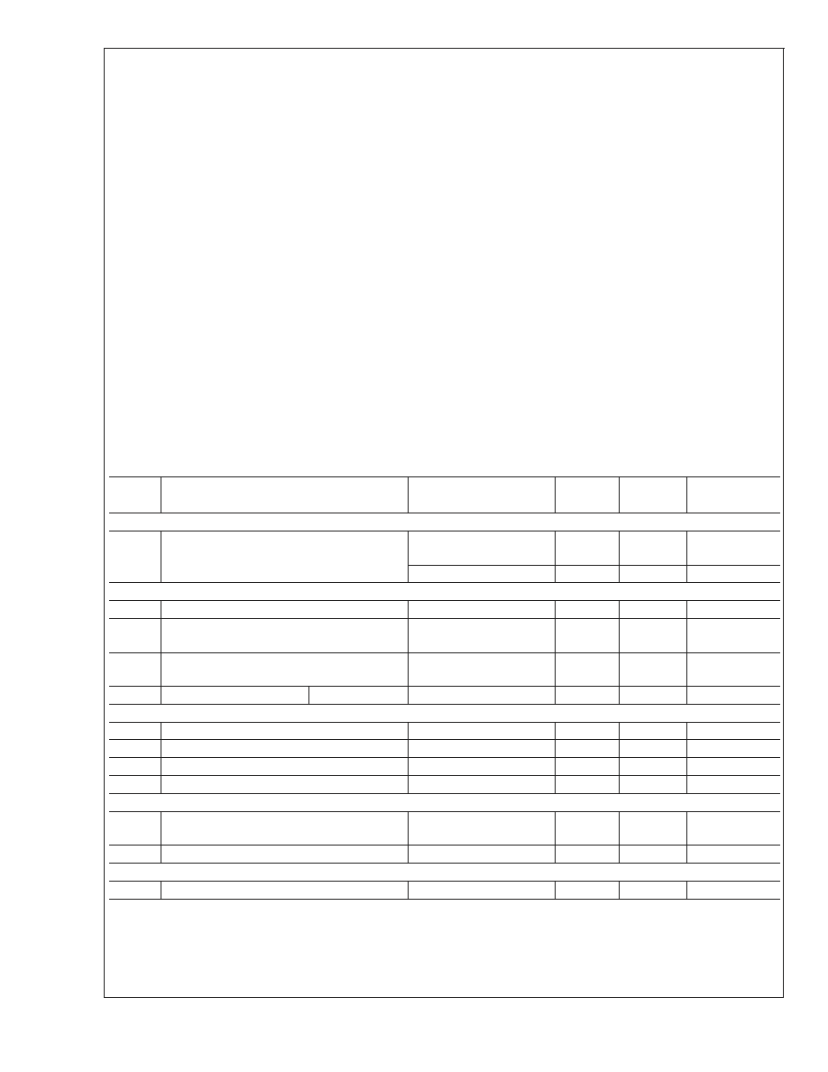
DC Electrical Characteristics
The following specifications apply for +2.8 V
DC
V
+
+3.8 V
DC
, Analog voltage inputs R
S
= 510
, unless otherwise speci-
fied. Boldface limits apply for T
A
= T
J
= T
MIN
to T
MAX
; all other limits T
A
= T
J
= 25 ∞C.(Note 8)
Symbol
Parameter
Conditions
Typical
Limits
Units
(Note 9)
(Note 10)
(Limits)
POWER SUPPLY CHARACTERISTICS
I
+
Supply Current
Normal Mode, Interface
Inactive
0.7
2.0
mA (max)
Shutdown Mode
0.5
mA
TEMPERATURE-TO-DIGITAL CONVERTER CHARACTERISTICS
Temperature Error using Internal Diode
±
3
∞C
Temperature Error using Remote Pentium
Diode Sensor (Note 11) and (Note 12)
0 ∞C
T
A
+125 ∞C, Vcc
= 3.3 Vdc
±
3
∞C (max)
Temperature Error using Remote 2N3904
Sensor (Note 11) and (Note 12)
-40 ∞C
T
A
+125 ∞C,
Vcc = 3.3 Vdc
±
4
∞C (max)
Resolution
8 bits
1.0
∞C (min)
LM87 ANALOG-TO-DIGITAL CONVERTER CHARACTERISTICS
Resolution
8
bits
TUE
Total Unadjusted Error
(Note 13)
±
2
% (max)
DNL
Differential Non-Linearity
±
1
LSB (max)
t
C
Total Monitoring Cycle Time
(Note 14)
0.28
sec
ADC INPUT CHARACTERISTICS
Input Resistance (All analog inputs except
AIN1 and AIN2)
130
90
k
(min)
AIN1 and AIN2 DC Input Current
12
µA
DAC CHARACTERISTICS
Resolution
8
Bits
LM87
www.national.com
4

DC Electrical Characteristics
(Continued)
The following specifications apply for +2.8 V
DC
V
+
+3.8 V
DC
, Analog voltage inputs R
S
= 510
, unless otherwise speci-
fied. Boldface limits apply for T
A
= T
J
= T
MIN
to T
MAX
; all other limits T
A
= T
J
= 25 ∞C.(Note 8)
Symbol
Parameter
Conditions
Typical
Limits
Units
(Note 9)
(Note 10)
(Limits)
DAC CHARACTERISTICS
DAC Error
0 ∞C
T
A
+75 ∞C, V
+
=
3.3 V, Code = 255
-3.3
% (min)
V
+
= 3.3 V, 3/4 Scale,
code 192
+3.7
%
0 ∞C
T
A
+75 ∞C, V, V
+
= 3.3 V, Code = 8(Note
15)
±
3
% (max)
R
L
Output Load Resistance
V
O
= 2.5 V
1250
(min)
C
L
Output Load Capacitance
20
pF (max)
FAN RPM-TO-DIGITAL CONVERTER
Fan RPM Error
+25 ∞C
T
A
+75 ∞C
±
10
% (max)
-10 ∞C
T
A
+100 ∞C
±
15
% (max)
-40 ∞C
T
A
+125 ∞C
±
20
% (max)
Full-scale Count
255
(max)
FAN1 and FAN2 Nominal Input
RPM (See Section 6.0)
Divisor = 1, Fan Count =
153 (Note 16)
8800
RPM
Divisor = 2, Fan Count =
153 (Note 16)
4400
RPM
Divisor = 3, Fan Count =
153 (Note 16)
2200
RPM
Divisor = 4, Fan Count =
153 (Note 16)
1100
RPM
DIGITAL OUTPUTS (NTEST_OUT)
V
OUT(1)
Logical "1" Output Voltage
I
OUT
=
±
3.0 mA at
V
+
= +2.8 V
2.4
V (min)
V
OUT(0)
Logical "0" Output Voltage
I
OUT
=
±
3.0 mA at
V
+
= +3.8 V
0.4
V (max)
OPEN- DRAIN DIGITAL OUTPUTS (SMBData, RESET#, CI, INT#, THERM#)
V
OUT(0)
Logical "0" Output Voltage (SMBData)
I
OUT
= -755 µA
0.4
V (min)
V
OUT(0)
Logical "0" Output Voltage (Others)
I
OUT
= -3 mA
0.4
V (min)
I
OH
High Level Output Current
V
OUT
= V
+
5
12
µA (max)
RESET# and Chassis Intrusion
45
20
ms (min)
Pulse Width
DIGITAL INPUTS: VID0≠VID4, NTEST_IN, ADD/NTEST_OUT, Chassis Intrusion (CI)
V
IN(1)
Logical "1" Input Voltage
2.0
V (min)
V
IN(0)
Logical "0" Input Voltage
0.8
V (max)
SMBus DIGITAL INPUTS (SMBCLK, SMBData)
V
IN(1)
Logical "1" Input Voltage
2.1
V (min)
V
IN(0)
Logical "0" Input Voltage
0.8
V (max)
V
HYST
Input Hysteresis Voltage
243
mV
Tach Pulse Logic Inputs (FAN1, FAN2)
V
IN(1)
Logical "1" Input Voltage
0.7 x V
+
V (min)
V
IN(0)
Logical "0" Input Voltage
0.3 x V
+
V (max)
ALL DIGITAL INPUTS
I
IN(1)
Logical "1" Input Current
V
IN
= V
+
-12
µA (min)
I
IN(0)
Logical "0" Input Current
V
IN
= 0 V
DC
12
µA (max)
C
IN
Digital Input Capacitance
20
pF
LM87
www.national.com
5