TL H 6744
LM9044
Lambda
Sensor
Interface
Amplifier
February 1995
LM9044 Lambda Sensor Interface Amplifier
General Description
The LM9044 is a precision differential amplifier specifically
designed for operation in the automotive environment Gain
accuracy is guaranteed over the entire automotive tempera-
ture range (
b
40 C to
a
125 C) and is factory trimmed prior
to package assembly The input circuitry has been specifi-
cally designed to reject common-mode signals as much as
3V below ground on a single positive power supply This
facilitates the use of sensors which are grounded at the
engine block while the LM9044 itself is grounded at chassis
potential An external capacitor sets the maximum operating
frequency of the amplifier thereby filtering high frequency
transients Both inputs are protected against accidental
shorting to the battery and against load dump transients
The input impedance is typically 1 MX
The output op amp is capable of driving capacitive loads
and is fully protected Also internal circuitry has been pro-
vided to detect open circuit conditions on either or both in-
puts and force the output to a ``home'' position (a ratio of
the external reference voltage)
Features
Y
Normal circuit operation guaranteed with inputs up to
3V below ground on a single supply
Y
Gain factory trimmed and guaranteed over temperature
(
g
3% of full-scale from
b
40 C to
a
125 C)
Y
Low power consumption (typically 1 mA)
Y
Fully protected inputs
Y
Input open circuit detection
Y
Operation guaranteed over the entire automotive tem-
perature range (
b
40 C to
a
125 C)
Y
Single supply operation
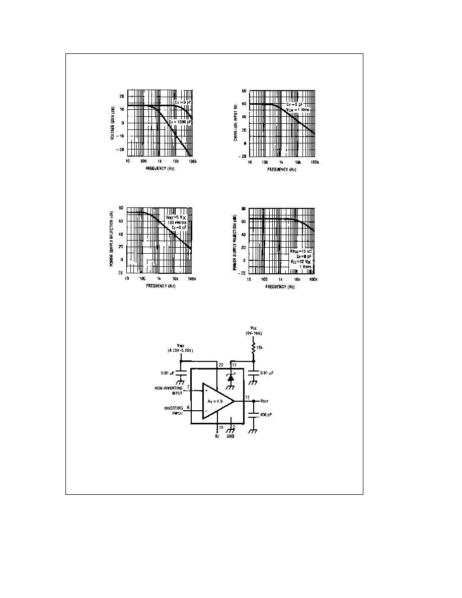
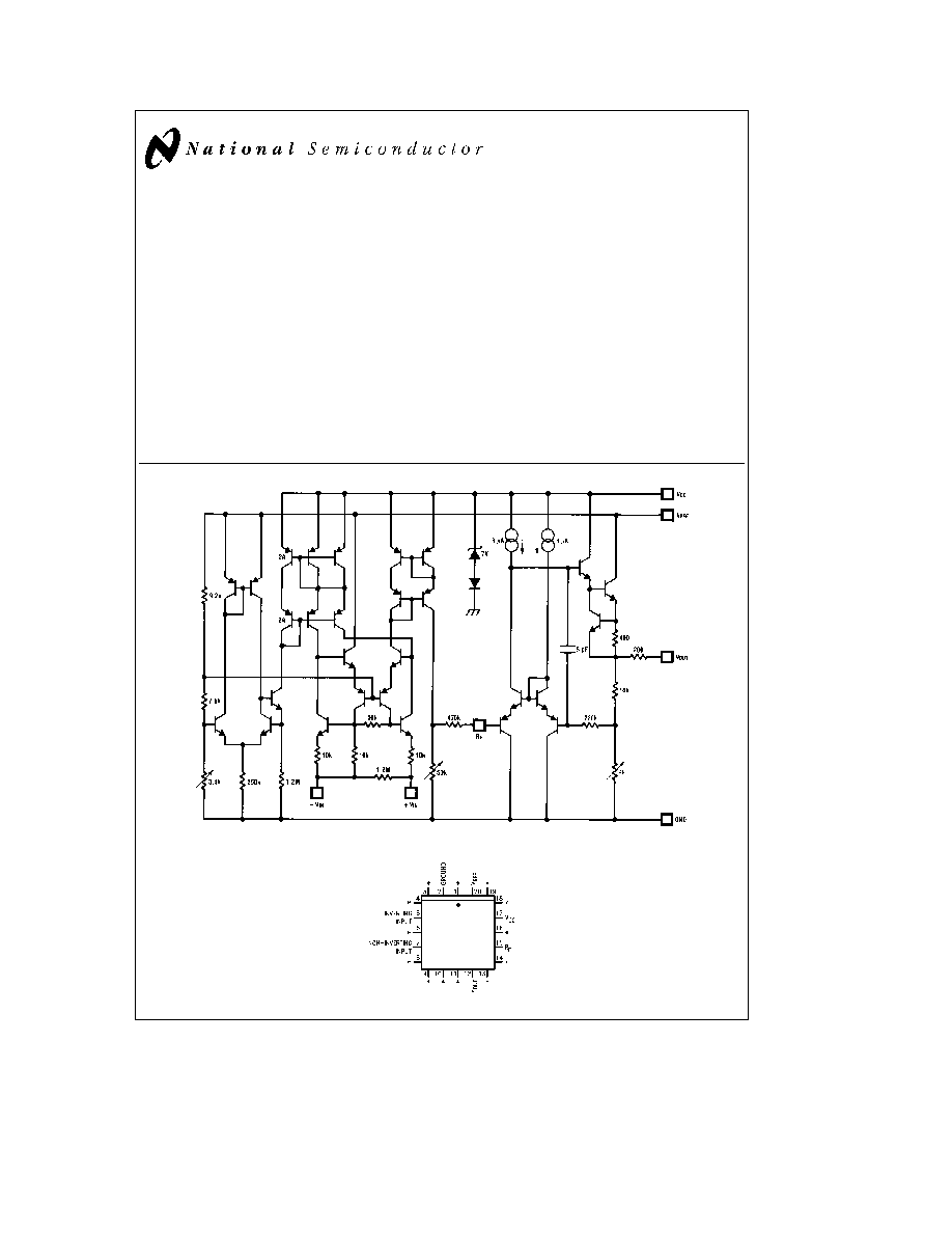
Schematic and Connection Diagrams
TL H 6744 1
Plastic Chip Carrier Package
Pins 1 3 4 6 8 9 10 11 13 14 16 18 19 are
trim pins and should be left floating
TL H 6744 6
Top View
Order Number LM9044V
See NS Package Number V20A
C1995 National Semiconductor Corporation
RRD-B30M115 Printed in U S A

Absolute Maximum Ratings
If Military Aerospace specified devices are required
please contact the National Semiconductor Sales
Office Distributors for availability and specifications
V
CC
Supply Voltage (RV
CC
e
15 kX)
g
60V
V
REF
Supply Voltage
b
0 3V to
a
6V
DC Input Voltage (Either Input)
b
3V to
a
16V
Input Transients (Note 1)
g
60V
Power Dissipation (see Note 6)
1350 mW
Output Short Circuit Duration
Indefinite
Operating Temperature Range
b
40 C to
a
125 C
Storage Temperature Range
b
65 C to
a
150 C
Soldering Information
Plastic Chip Carrier Package
Vapor Phase (60 seconds)
215 C
Infrared (15 seconds)
220 C
See AN-450 ``Surface Mounting Methods and Their Effect
on Product Reliability'' for other methods of soldering sur-
face mount devices
Electrical Characteristics
V
CC
e
12V V
REF
e
5V
b
40 C
s
T
A
s
125 C unless otherwise noted
Parameter
Conditions
(Note 2)
(Note 3)
Units
Min
Typ
Max
Min
Typ
Max
Differential Voltage Gain
V
DIF
e
0 5V
4 41
4 50
4 59
V V
b
1V
s
V
CM
s
a
1V
V
DIF
e
0 5V
b
3V
s
V
CM
s
a
1V
4 36
4 50
4 64
V V
Gain Error (Note 5)
0
s
V
DIF
s
1V
b
2
0
2
% FS
b
1V
s
V
CM
s
a
1V
0
s
V
DIF
s
1V
b
3
0
3
% FS
b
3V
s
V
CM
s
a
1V
Differential Input Resistance
o
s
V
DIF
s
1V
0 95
1 20
3 00
MX
b
1V
s
V
CM
s
a
1V
0
s
V
DIF
s
1V
0 70
1 20
4 00
MX
b
3V
s
V
CM
s
a
1V
Non-Inverting Input Bias
0
s
V
DIF
s
1V
g
0 38
g
0 65
m
A
Current
b
1V
s
V
CM
s
a
1V
0
s
V
DIF
s
1V
g
0 38
g
1 5
m
A
b
3V
s
V
CM
s
a
1V
Inverting Input Bias Current
0
s
V
DIF
s
1V
b
25
b
65
b
100
m
A
b
1V
s
V
CM
s
a
1V
0V
s
V
DIF
s
1V
b
45
b
150
m
A
b
3V
s
V
CM
s
a
1V
V
CC
Supply Current
V
CC
e
12V RV
CC
e
15k
300
500
m
A
V
REF
Supply Current
4 75V
s
V
REF
s
5 5V
0 5
1 0
mA
Common-Mode Voltage
b
1
1
b
3
1
V
Range (Note 4)
DC Common-Mode
Input Referred
50
60
dB
Rejection Ratio
b
1V
s
V
CM
s
a
1V
V
DIF
e
0 5V
Open Circuit Output Voltage
One or Both Inputs
0 371
0 397
0 423
XV
REF
Open
b
1V
s
V
CM
s
a
1V
b
3V
s
V
CM
s
a
1V
0 365
0 397
0 429
XV
REF
Short Circuit Output Current
Output Grounded
1 0
2 7
5 0
mA
V
CC
Power Supply Rejection
V
CC
e
12V RV
CC
e
15K
50
65
dB
Ratio
V
DIF
e
0 5V
V
REF
Power Supply
V
REF
e
5 V
DC
60
74
dB
Rejection Ratio
V
DIF
e
0 5V
Note 1
This test is performed with a 1000X source impedance
Note 2
These parameters are guaranteed and 100% production tested
Note 3
These parameters will be guaranteed but not 100% production tested
Note 4
The LM9044 has been designed to common-mode to
b
3V but production testing is only performed at
g
1V
Note 5
Gain error is given as a percent of full-scale Full-scale is defined as 1V at the input and 4 5V at the output
Note 6
For operation in ambient temperatures above 25 C the device must be derated based on a maximum junction temperature of 150 C and a thermal
resistance of 93 C W junction to ambient
2
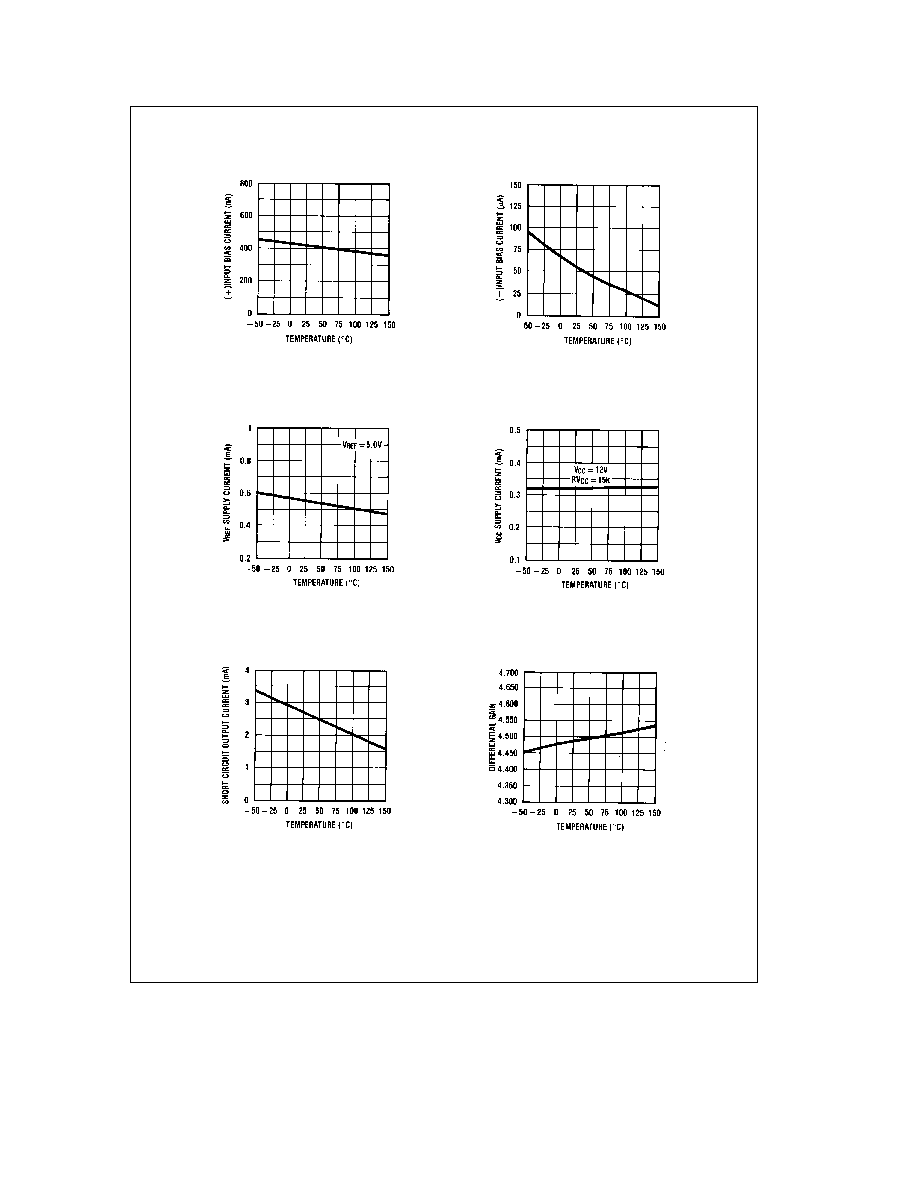
Typical Performance Characteristics
Non-Inverting Input Bias
Current vs Temperature
Inverting Input Bias Current
vs Temperature
V
REF
Supply Current vs
Temperature
V
CC
Supply Current vs
Temperature
Short Circuit Output
Current vs Temperature
Differential Gain vs
Temperature
TL H 6744 3
3