
LM95010
Digital Temperature Sensor with SensorPath
TM
Bus in
MSOP8 Package
General Description
The LM95010 is a digital output temperature sensor that has
single-wire interface compatible with National Semiconduc-
tor's SensorPath interface. It uses a
V
be
analog tempera-
ture sensing technique that generates a differential voltage
that is proportional to temperature. This voltage is digitized
using
a
Sigma-Delta
analog-to-digital
converter.
The
LM95010 is part of a hardware monitor system, comprised of
two parts: the PC System Health Controller (Master), such
as a Super I/O, and up to seven slaves of which four can be
LM95010s. Using SensorPath, the LM95010 will be con-
trolled by the master and report to the master its own die
temperature. SensorPath data is pulse width encoded,
thereby allowing the LM95010 to be easily connected to
many general purpose micro-controllers.
Features
n
SensorPath Bus
-- 4 hardware programmable addresses
n
Temperature Sensing
-- 0.25 ∞C resolution
-- 127.75 ∞C maximum temperature reading
n
8-lead MSOP package
Key Specifications
n
Temperature Sensor Accuracy
±
2 ∞C (max)
n
Temperature Range
-20 ∞C to +125 ∞C
n
Power Supply Voltage
+3.0V to +3.6V
n
Power Supply Current
0.5 mA (typ)
n
Conversion Time
14 ms to 1456 ms
Applications
n
Microprocessor based equipment
-- (Motherboards, Base-stations, Routers, ATMs, Point
of Sale, ...)
n
Power Supplies
Block Diagram
20082001
SensorPath
TM
is a trademark of National Semiconductor Corporation.
November 2003
LM95010
Digital
T
emperature
Sensor
with
SensorPath
Bus
in
MSOP8
Package
© 2003 National Semiconductor Corporation
DS200820
www.national.com
Connection Diagram
20082002
Ordering Information
Order
Number
Package
Marking
NS
Package
Number
Transport
Media
LM95010CIMM
T19C
MUA08A 1000 units in
tape and reel
LM95010CIMMX
T19C
MUA08A 3500 units in
tape and reel
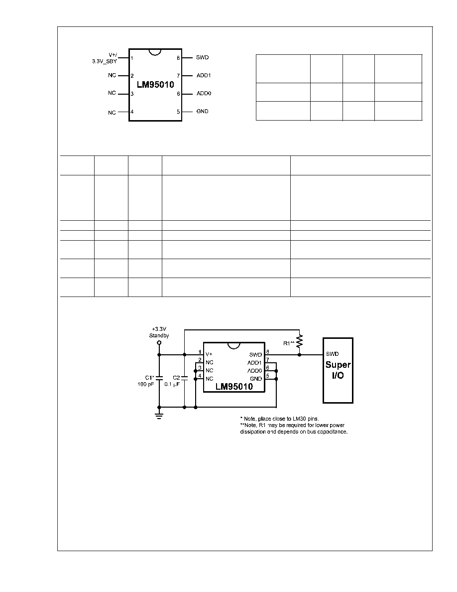
Pin Description
Pin
Number
Pin Name
Type
Description
Typical Connection
1
V+/3.3V
SB
Power
Positive power supply pin +3.3V pin.
Should be powered by +3.3V Standby power.
This pin should be bypassed with a 0.1 µF
capacitor. A bulk capacitance of approximately
10 µF needs to be in the near vicinity of the
LM95010.
2-4
NC
Must be grounded.
5
GND
Power
Ground
System ground
6
ADD0
Input
Address select input that assigns the serial
bus device number
10k resistor to V+ or GND; must never be left
floating
7
ADD1
Input
Address select input that assigns the serial
bus device number
10k resistor to V+ or GND; must never be left
floating
8
SWD
Input/
Output
Single-wire Data, SensorPath serial
interface line; Open-drain output
Super I/O with 1.25k pull-up to 3.3V
Typical Application
20082003
FIGURE 1. LM95010 connection to SensorPath master such as a Super I/O.
LM95010
www.national.com
2

Absolute Maximum Ratings
(Notes 1, 2)
Supply Voltage (V
+
)
-0.5 V to 6.0 V
Voltage on Pin 2
-0.3 V to (V+ + 0.3 V)
Voltage on all other Pins
-0.5 V to 6.0 V
Input Current per Pin(Note 3)
5 mA
Package Input Current (Note 3)
30 mA
Package Power Dissipation
(Note 5)
Output Sink Current
10 mA
Storage Temperature
-65 ∞C to +150 ∞C
ESD Susceptibility (Note 4)
Human Body Model
2000 V
Machine Model
200 V
Soldering Information, Lead Temperature
MSOP-8 Package (Note 6)
Vapor Phase (60 seconds)
215 ∞C
Infrared (15 seconds)
220 ∞C
Operating Ratings
(Notes 1, 2)
Temperature Range for
Electrical Characteristics
T
MIN
T
A
T
MAX
LM95010CIMM
-20 ∞C
T
A
+125 ∞C
Operating Temperature Range
-20 ∞C
T
A
+125 ∞C
Supply Voltage Range (V+)
+3.0 V to +3.6 V
DC Electrical Characteristics
The following specifications apply for V+ = 3.0 V
DC
to 3.6 V
DC
, unless otherwise specified in the conditions. Boldface limits
apply for T
A
= T
J
= T
MIN
to T
MAX
; all other limits T
A
= +25 ∞C.
POWER SUPPLY CHARACTERISTICS
Symbol
Parameter
Conditions
Typical
(Note 7)
Limits
(Note 8)
Units
(Limit)
V+
Power Supply Voltage
3.3
3.0
3.6
V (min)
V (max)
I+
AVG
Average Power Supply Current
SensorPath Bus Inactive (Note
9)
500
750
µA (max)
I+
Peak
Peak Power Supply Current
SensorPath Bus Inactive (Note
9)
1.6
mA
Power-On Reset Threshold Voltage
1.6
V (min)
2.8
V (max)
TEMPERATURE-TO-DIGITAL CONVERTER CHARACTERISTICS
Parameter
Conditions
Typical
(Note 7)
Limits
(Note 8)
Units
(Limits)
Temperature Error
T
A
= -20 ∞C and +125 ∞C (Note 10)
±
1
±
3
∞C (max)
+25 ∞C
T
A
+60 ∞C (Note 10)
±
2
∞C (max)
Temperature Resolution
10
Bits
0.25
∞C
SWD and ADD DIGITAL INPUT CHARACTERISTICS
Symbol
Parameter
Conditions
Typical
(Note 7)
Limits
(Note 8)
Units
(Limit)
V
IH
SWD Logical High Input Voltage
2.1
V (min)
V+ + 0.5
V (max)
V
IL
SWD Logical Low Input Voltage
0.8
V (max)
T
A
= 0 ∞C to +85 ∞C
-0.5
V (min)
-0.3
V (min)
V
IH
ADD Logical High Input Voltage
90% x V+
V (min)
V
IL
ADD Logical Low Input Voltage
10% x V+
V (max)
V
HYST
SWD Input Hysteresis
300
mV
I
L
SWD and ADD Input Leakage
Current
GND
V
IN
V+
±
0.005
±
10
µA (max)
SWD Input Leakage Current with V+
Open or Grounded
GND
V
IN
3.6 V,
and V+ Open or
GND
±
0.005
µA
LM95010
www.national.com
3

SWD and ADD DIGITAL INPUT CHARACTERISTICS
Symbol
Parameter
Conditions
Typical
(Note 7)
Limits
(Note 8)
Units
(Limit)
C
IN
Digital Input Capacitance
10
pF
SWD DIGITAL OUTPUT CHARACTERISTICS
Symbol
Parameter
Conditions
Typical
(Note 7)
Limits
(Note 8)
Units
(Limit)
V
OL
Open-drain Output Logic "Low"
Voltage
I
OL
= 4 mA
0.4
V (max)
I
OL
= 50 µA
0.2
V (max)
I
OH
Open-drain Output Off Current
±
0.005
±
10
µA (max)
C
OUT
Digital Output Capacitance
10
pF
AC Electrical Characteristics
The following specification apply for V+ = +3.0V
DC
to +3.6V
DC
, unless otherwise specified. Boldface limits apply for
T
A
= T
J
= T
MIN
to T
MAX
; all other limits T
A
= T
J
= 25 ∞C. The SensorPath Characteristics conform to the SensorPath specifi-
cation. Please refer to that specification for further details.
HARDWARE MONITOR CHARACTERISTICS
Symbol
Parameter
Conditions
Typical
(Note 7)
Limits
(Note 8)
Units
(Limits)
t
CONV
Total Monitoring Cycle Time (Note 11)
Default
182
163.8
ms (min)
200.2
ms (max)
SensorPath Bus CHARACTERISTICS
Symbol
Parameter
Conditions
Typical
(Note 7)
Limits
(Note 8)
Units
(Limits)
t
f
SWD fall time (Note 12)
R
pull-up
= 1.25 k
±
30%, C
L
= 400 pF
300
ns (max)
t
r
SWD rise time (Note 13)
R
pull-up
=
1.25 k
±
30%,
C
L
= 400 pF
1000
ns (max)
t
INACT
Minimum inactive time (bus at high level)
guaranteed by the LM95010 before an
Attention Request
11
µs (min)
t
Mtr0
Master drive for Data Bit 0 write and for
Data Bit 0-1read
11.8
µs (min)
17.0
µs (max)
t
Mtr1
Master drive for Data Bit 1 write
35.4
µs (min)
48.9
µs (max)
t
SFEdet
Time allowed for LM95010 activity
detection
9.6
µs (max)
t
SLout1
LM95010 drive for Data Bit 1 read by
master
28.3
µs (min)
38.3
µs (max)
t
MtrS
Master drive for Start Bit
80
µs (min)
109
µs (max)
t
SLoutA
LM95010 drive for Attention Request
165
µs (min)
228
µs (max)
t
RST
Master or LM95010 drive for Reset
354
µs (min)
t
RST_MAX
Maximum drive of SWD by an LM95010,
after the power supply is raised above 3V
500
ms (max)
LM95010
www.national.com
4

20082004
FIGURE 2. Timing for Data Bits 0, 1 and Start Bit. See Section 1.2 "Bit Signaling" for further details.
LM95010
www.national.com
5