 | –≠–ª–µ–∫—Ç—Ä–æ–Ω–Ω—ã–π –∫–æ–º–ø–æ–Ω–µ–Ω—Ç: LM9811 | –°–∫–∞—á–∞—Ç—å:  PDF PDF  ZIP ZIP |
LM9811
10-Bit Greyscale/30-Bit Color
Linear CCD Sensor Processor
General Description
The LM9811 is a high performance integrated signal
processor/digitizer for linear CCD image scanners. The
LM9811 performs all the analog processing (correlated
double sampling for black level and offset compensation,
pixel-by-pixel
gain
(shading)
correction,
and
10-bit
analog-to-digital conversion) necessary to maximize the per-
formance of a wide range of linear CCD sensors.
The LM9811 can be digitally programmed to work with a
wide variety of CCDs from different manufacturers. An inter-
nal configuration register sets CCD and sampling timing to
maximize performance, simplifying the design and manufac-
turing processes.
The LM9811 can be used with parallel output color CCDs. A
signal inversion mode eases use with CIS sensors. For
complementary voltage reference see the LM4041.
Applications
n
Color and Greyscale Flatbed and Sheetfed Scanners
n
Fax and Multifunction Peripherals
n
Digital Copiers
n
General Purpose Linear CCD Imaging
Features
n
1.5 Million pixels/s conversion rate
n
Pixel-rate shading correction for individual pixels
maximizes dynamic range and resolution, even on
"weak" pixels
n
Implements Correlated Double Sampling for minimum
noise and offset error
n
Reference and signal sampling points digitally controlled
in 40ns increments for maximum performance
n
Generates all necessary CCD clock signals
n
Compatible with a wide range of linear CCDs
n
Supports some Contact Image Sensors (CIS)
n
TTL/CMOS input/output compatible
Key Specifications
n
Resolution:
10 Bits
n
Pixel Conversion Rate:
1.5MHz
n
Supply Voltage:
+5V
±
5%
n
Supply Voltage
(Digital I/O):
+3.3V
±
10% or +5V
±
5%
n
Power Dissipation:
260mW (max)
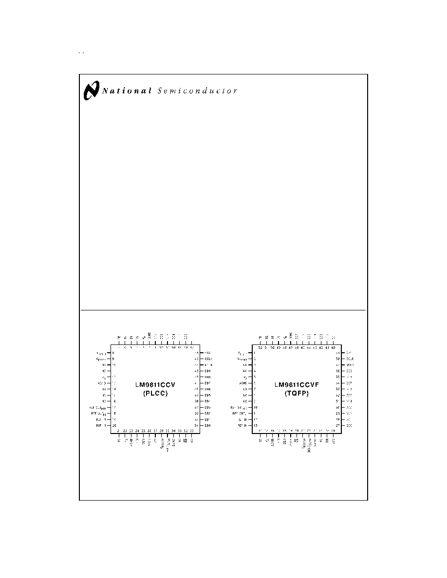
Connection Diagrams
TRI-STATE
Æ
is a registered trademark of National Semiconductor Corporation.
MICROWIRE
TM
is a trademark of National Semiconductor Corporation.
SPI
TM
is a trademark of Motorola, Inc.
DS012813-1
DS012813-2
April 1998
LM981
1
10-Bit
Greyscale/30-Bit
Color
Linear
CCD
Sensor
Processor
© 1999 National Semiconductor Corporation
DS012813
www.national.com
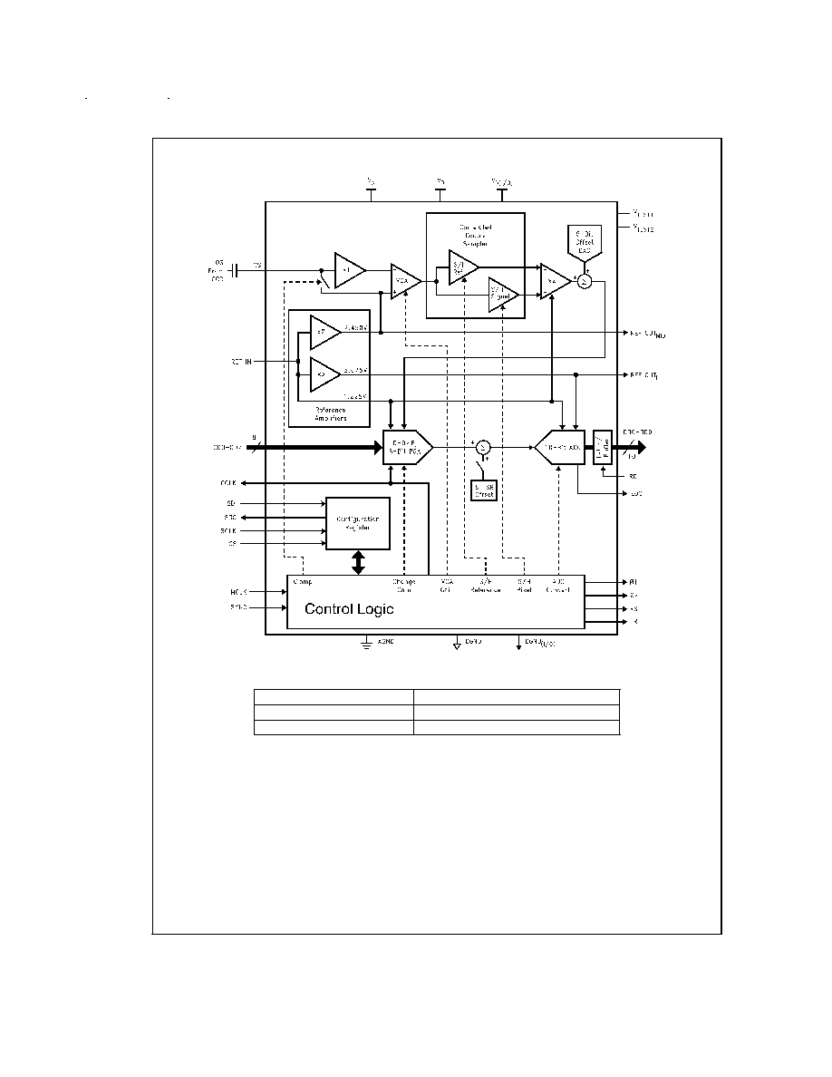
Block Diagram
Ordering Information
Commercial (0∞C
T
A
+70∞C)
Package
LM9811CCV
V52A 52-Pin Plastic Leaded Chip Carrier
LM9811CCVF
VEG52A 52-Pin Thin Quad Flatpack
DS012813-3
www.national.com
2
Absolute Maximum Ratings
(Notes 1, 2)
Positive Supply Voltage (V
+
= V
A
= V
D
= V
D(I/O
)
with Respect to
GND = AGND = DGND = DGND
(I/O)
6.5V
Voltage on any Input or Output Pin
0.3V to V
+
+0.3V
Input Current at any Pin (Note 3)
±
25 mA
Package Input Current (Note 3)
±
50 mA
Package Dissipation at T
A
= 25∞C
(Note 4)
ESD Susceptibility (Note 5)
Human Body Model
2000V
Soldering Information (Note 6)
Infrared, 10 seconds
LM9811CCV
300∞C
LM9811CCVF
220∞C
Storage Temperature
-65∞C to +150∞C
Operating Ratings
(Notes 1, 2)
Operating Temperature
Range
T
MIN
T
A
T
MAX
LM9811CCV, LM9811CCVF
0∞C
T
A
+70∞C
V
A
Supply Voltage
+4.75V to +5.25V
V
D
Supply Voltage
+4.75V to +5.25V
V
D(I/O)
Supply Voltage
+2.7V to +5.25V
|V
A
≠V
D
|
100 mV
V
A
≠V
D(I/O)
-100 mV
OS, REF IN Voltage Range
-0.05V to V
A
+ 0.05V
CD0≠CD7, MCLK, SYNC,
SDI, SCLK, CS, RD,
Voltage Range
-0.05V to V
D(I/O)
+ 0.05V
Electrical Characteristics
The following specifications apply for AGND = DGND = DGND(I/O) = 0V, V
A
= V
D
= +5.0V
DC
, V
D(I/O)
= +5.0 or +3.0V
DC
,
REF IN = +1.225V
DC
, f
MCLK
= 20MHz, R
S
= 25
. All LSB units are ADC LSBs unless otherwise specified. Boldface limits
apply for T
A
= T
J
= T
MIN
to T
MAX
; all other limits T
A
= T
J
= 25∞C. (Note 8)
Symbol
Parameter
Conditions
Typical
Limits
Units
(Note 9)
(Note 10)
(Limits)
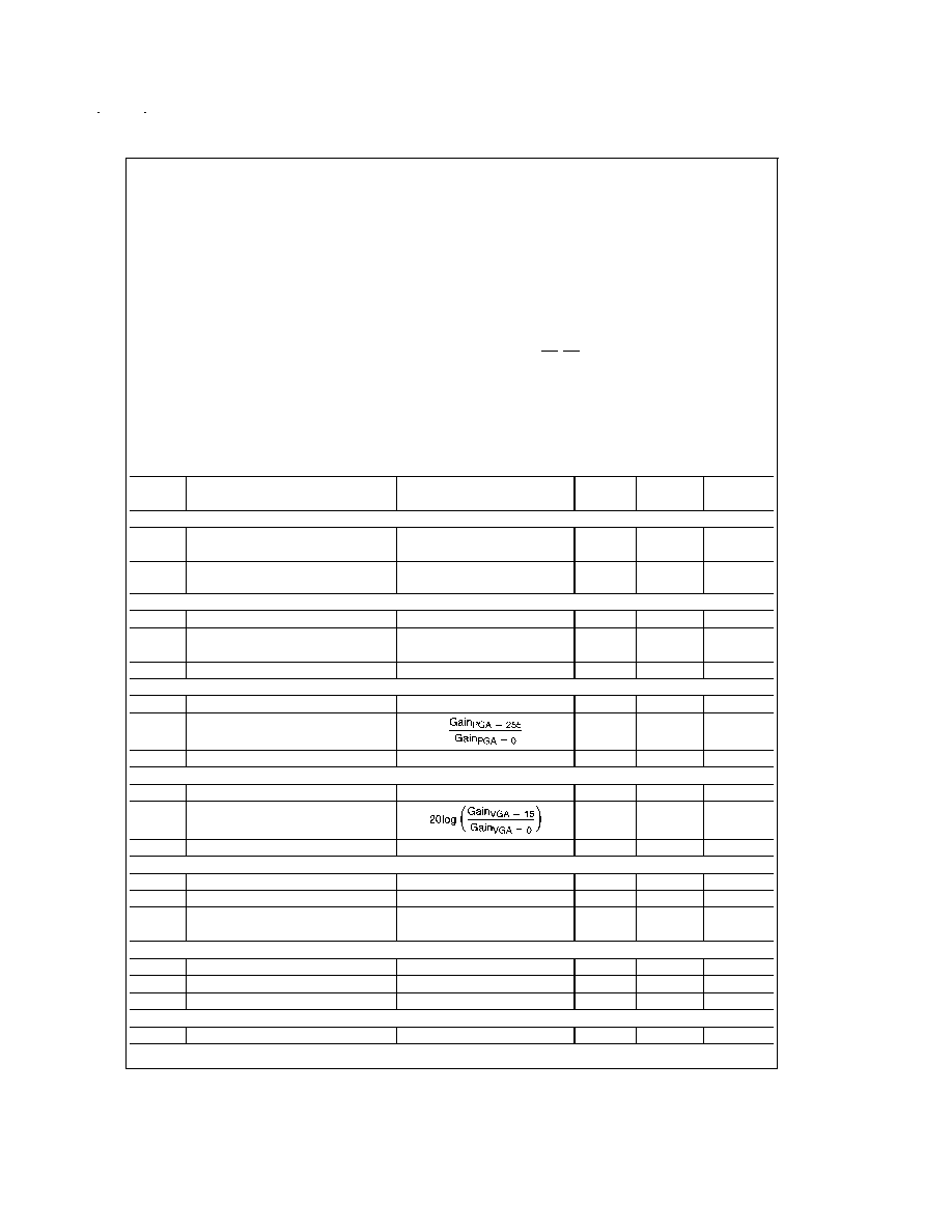
CCD SOURCE REQUIREMENTS FOR FULL SPECIFIED ACCURACY AND DYNAMIC RANGE (Note 11)
V
WHITE
Maximum Peak CCD Differential
VGA Gain = 0 dB
1.1
V (min)
Signal Range
VGA Gain = 9 dB
0.4
V (min)
V
RFT
Maximum CCD Reset FeedThrough
Amplitude
2
V (min)
ADC CHARACTERISTICS (Note 16)
Resolution with No Missing Codes
f
MCLK
= 12MHz
9
Bits (min)
ILE
Integral Linearity Error (Note 12)
f
MCLK
= 12MHz
+4.0
LSB (max)
-3.0
LSB (min)
DNL
Differential Non-Linearity
f
MCLK
= 12MHz
+2.0
LSB (max)
PGA CHARACTERISTICS
Monotonicity
8
Bits (min)
PGA Adjustment Range
2.95
2.8
V/V (min)
Gain Error at any Gain (Note 14)
1.4
% (max)
VGA CHARACTERISTICS
Monotonicity
4
Bits (min)
VGA Adjustment Range
8.95
8.5
dB (min)
Gain Error at any Gain (Note 15)
±
0.15
dB (max)
OFFSET TRIM CHARACTERISTICS
Offset DAC LSB Size
In Units of ADC LSBs
1.7
LSB
Offset DAC DNL
In Units of Offset DAC LSBs
±
0.25
±
0.9
LSB
Offset Add Magnitude
In Units of ADC LSBs
8
6.4
LSB (min)
10.0
LSB (max)
SYSTEM CHARACTERISTICS
Full Channel Gain Error
VGA Gain = 1, PGA Gain = 1
±
0.6
±
3.0
% (max)
Pre-PGA Offset Error (In ADC LSBs)
VGA Gain = 1, Offset DAC = 0
±
4
LSB
Post-PGA Offset Error (In ADC LSBs)
Offset Add = 0
±
4
LSB
REFERENCE AND ANALOG INPUT CHARACTERSTICS (Note 7)
OS Input Capacitance
5
pF
www.national.com
3
Electrical Characteristics
(Continued)
The following specifications apply for AGND = DGND = DGND(I/O) = 0V, V
A
= V
D
= +5.0V
DC
, V
D(I/O)
= +5.0 or +3.0V
DC
,
REF IN = +1.225V
DC
, f
MCLK
= 20MHz, R
S
= 25
. All LSB units are ADC LSBs unless otherwise specified. Boldface limits
apply for T
A
= T
J
= T
MIN
to T
MAX
; all other limits T
A
= T
J
= 25∞C. (Note 8)
Symbol
Parameter
Conditions
Typical
Limits
Units
(Note 9)
(Note 10)
(Limits)
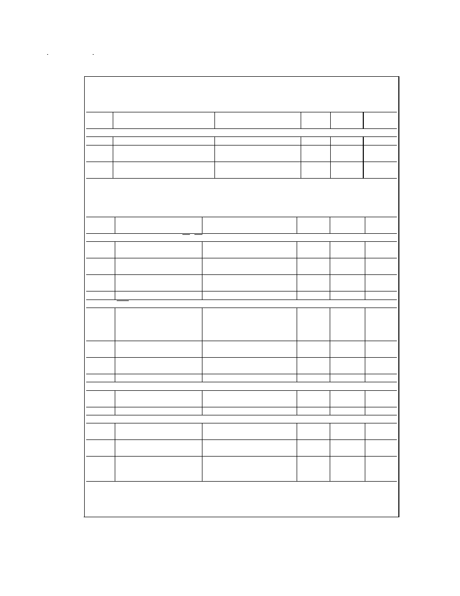
REFERENCE AND ANALOG INPUT CHARACTERSTICS (Note 7)
OS Input Leakage Current
Measured with OS = 2.45V
DC
2
20
nA (max)
R
REF
ADC Reference Ladder (REF OUT
HI
950
500
(min)
to REF IN) Impedance
2000
(max)
REF IN
Reference Voltage (Note 13)
1.225
1.19
V (min)
1.26
V (max)
DC and Logic Electrical Characteristics
The following specifications apply for AGND = DGND = DGND
(I/O)
= 0V, V
A
= V
D
= +5.0V
DC
, V
D(I/O)
= +5.0 or +3.0V
DC
, REF
IN = +1.225V
DC
, f
MCLK
= 20MHz, R
s
= 25
. Boldface limits apply for T
A
= T
J
= T
MIN
to T
MAX
; all other limits T
A
= T
J
=
25∞C.
Symbol
Parameter
Conditions
Typical
Limits
Units
(Note 9)
(Note 10)
(Limits)
CD0≠CD7, MCLK, SYNC, SDI, SCLK, CS , RD DIGITAL INPUT CHARACTERISTICS
V
IN(1)
Logical "1" Input Voltage
V
D(I/O)
= 5.25V
2.0
V (min)
V
D(I/O)
= 3.6V
2.0
V (min)
V
IN(0)
Logical "0" Input Voltage
V
D(I/O)
= 4.75V
0.8
V (max)
V
D(I/O)
= 2.7V
0.7
V (max)
I
IN
Input Leakage Current
V
IN
= V
D
0.1
µA
V
IN
= DGND
-0.1
µA
C
IN
Input Capacitance
5
pF
DD0≠DD9, EOC , CCLK, SDO DIGITAL OUTPUT CHARACTERISTICS
V
OUT(1)
Logical "1" Output Voltage
V
D(I/O)
= 4.75V, I
OUT
= -360 µA
2.4
V (min)
V
D(I/O)
= 4.75V, I
OUT
= -10 µA
4.4
V (min)
V
D(I/O)
= 2.7V, I
OUT
= -360 µA
2.1
V (min)
V
D(I/O)
= 2.7V, I
OUT
= -10 µA
2.5
V (min)
V
OUT(0)
Logical "0" Output Voltage
V
D(I/O)
= 5.25V, I
OUT
= 1.6 mA
0.4
V (max)
V
D(I/O)
= 3.6V, I
OUT
= 1.6 mA
0.4
V (max)
I
OUT
TRI-STATE
Æ
Output Current
V
OUT
= DGND
0.1
µA
(DD0≠DD9 only)
V
OUT
= V
D
-0.1
µA
C
OUT
TRI-STATE Output Capacitance
5
pF
1,
2, RS, TR DIGITAL OUTPUT CHARACTERISTICS
V
OUT(1)
Logical "1" Output Voltage
V
D
= 4.75V, I
OUT
= -360 µA
2.4
V (min)
V
D
= 4.75V, I
OUT
= -10 µA
4.4
V (min)
V
OUT(0)
Logical "0" Output Voltage
V
D
= 5.25V, I
OUT
= 1.6 mA
0.4
V (max)
POWER SUPPLY CHARACTERISTICS
I
A
Analog Supply Current
Operating
25
38
mA (max)
Standby
50
µA
I
D
Digital Supply Current
Operating
6
8
mA (max)
Standby
65
µA
I
D(I/O)
Digital I/O Supply Current
Operating, V
D(I/O)
= 5.0V
3.1
6
mA (max)
Operating, V
D(I/O)
= 3.0V
1.6
4
mA (max)
Standby, V
D(I/O)
= 5.0V or 3.0V
1.7
mA
www.national.com
4
AC Electrical Characteristics, MCLK Independent
The following specifications apply for AGND = DGND = DGND
(I/O)
= 0V, V
A
= V
D
= V
D(I/O)
= +5.0V
DC
, REF IN = +1.225V
DC
,
f
MCLK
= 20MHz, t
MCLK
= 1/f
MCLK
, t
r
= t
f
= 5ns, R
s
= 25
, C
L
(databus loading) = 50 pF/pin. Boldface limits apply for T
A
= T
J
= T
MIN
to T
MAX
; all other limits T
A
= T
J
= 25∞C.
Symbol
Parameter
Conditions
Typical
Limits
Units
(Note 9)
(Note 10)
(Limits)
f
MCLK
Maximum MCLK Frequency (Note 16)
20
MHz (min)
Minimum MCLK Frequency
1
MHz (max)
MCLK Duty Cycle
30
40
% (min)
70
60
% (max)
t
A
SYNC Setup of MCLK
5
10
ns (min)
t
CDSETUP
Correction Data Valid to CLK Setup
14
20
ns (min)
t
CDHOLD
Correction Data Valid to CLK Hold
-12
0
ns (min)
t
D1H
, t
D0H
RD High to DD0≠DD9 TRI-STATE
5
15
ns (max)
t
DACC
Access Time Delay from RD Low to
DD0≠DD9 Data Valid
15
30
ns (max)
f
SCLK
Maximum SCLK Frequency
8
MHz (min)
SCLK Duty Cycle
40
% (min)
60
% (max)
t
SDI
SDI Set-Up Time from SCLK
Rising Edge
3
10
ns (min)
t
HDI
SDI Hold Time from SCLK
Rising Edge
2
15
ns (min)
t
DDO
Delay from SCLK Falling Edge to
SDO Data Valid
25
55
ns (max)
t
HDO
SDO Hold Time from SCLK
Falling Edge
R
L
= 3k, C
L
= 25pF
30
55
ns (max)
5
ns (min)
t
DELAY
DELAY from SCLK Falling Edge to CS
Rising or Falling Edge
5
10
ns (min)
t
SETUP
Set-Up Time of CS Rising or Falling
Edge to SCLK Rising Edge
0
10
ns (min)
t
S1H
, t
S0H
Delay from CS Rising Edge to SDO
TRI-STATE
R
L
= 3k, C
L
= 50pF
25
50
ns (max)
t
RDO
SDO Rise Time, TRI-STATE to High
R
L
= 3k, C
L
= 50pF
20
ns
SDO Rise Time, Low to High
20
ns
t
FDO
SDO Fall Time, TRI-STATE to Low
R
L
= 3k, C
L
= 50pF
20
ns
SDO Fall Time, High to Low
20
ns
AC Electrical Characteristics, MCLK Dependent
The following specifications apply for AGND = DGND = DGND
(I/O)
= 0V, V
A
= V
D
= V
D(I/O)
= +5.0V
DC
, REF IN = +1.225V
DC
,
f
MCLK
= 20MHz, t
MCLK
= 1/f
MCLK
, t
r
= t
f
= 5ns, R
s
= 25
, C
L
(databus loading) = 50 pF/pin. Refer to
Table 2. Configuration
Register Parameters for limits labelled C.R. Boldface limits apply for T
A
= T
J
= T
MIN
to T
MAX
; all other limits T
A
= T
J
=
25∞C.
Symbol
Parameter
Conditions
Typical
Limits
Units
(Note 9)
(Note 10)
(Limits)
t
START
MCLK to first
1 High
50ns
1
t
MCLK
t
1,
2 Clock Period
Standard CCD Mode
400ns
8
t
MCLK
Even/Odd CCD Mode
800ns
16
t
MCLK
t
TRWIDTH
Transfer Pulse (TR) Width
C.R.
µs
t
GUARD
1 to TR, TR to
1 Guardband
C.R.
ns
t
RSWIDTH
Reset Pulse (RS) Width
C.R.
ns
t
RS
Falling Edge of
1 to RS
Standard CCD Mode
C.R.
ns
Either Edge of
1 to RS
Even/Odd CCD Mode
www.national.com
5