Äîêóìåíòàöèÿ è îïèñàíèÿ www.docs.chipfind.ru
© 2000
National Semiconductor Corporation
www.national.com
N
LM98503
10-Bit, 18 MSPS Camera Signal Processor
General Description
The LM98503 is a CCD signal processor for digital cameras.
The processor provides a common interface to a number of
different image sensors including CCD, CMOS, and CIS.
Correlated double sampling reduces kTC noise from the image
signal. A fast, temperature stable, 8-bit digitally programmable
gain amplifier enables pixel-rate white-balancing. An auxiliary
input is provided, allowing for the selection of an external signal,
useful for sampling analog video signals. The 10-bit A/D
converter preserves the image quality with excellent noise
performance. The LM98503 also includes the supporting
functions of digital black level clamp and power down, ideally
suited for portable video applications. This low-power processor
is a natural choice for the most demanding imaging systems.
Applications
!
!
!
!
Digital still cameras
!
!
!
!
Digital video camcorders
!
!
!
!
Video conferencing
!
!
!
!
Security cameras
!
!
!
!
Plain paper copiers
!
!
!
!
Flatbed or handheld color scanners
!
!
!
!
Video processing for X-ray or infrared
!
!
!
!
Barcode scanners
Features
!
!
!
!
+3 Volt single power supply
!
!
!
!
Low power CMOS design
!
!
!
!
4-Wire serial interface
!
!
!
!
2.5V data output voltage swing
!
!
!
!
AUX input with analog clamp and programmable gain
!
!
!
!
Four color gain and offset registers
!
!
!
!
Digital black level clamp
!
!
!
!
Small 48-lead LQFP package
!
!
!
!
Supports interlace and progressive scan CCDs.
Key Specifications
* Note:
20 log
10
(V
IN
/ RMS Output Noise)
!
Maximum Input Level
1.0 Volt peak-peak
!
CDS Sampling Rate
18 MSPS
!
PGA Gain Steps
256 Steps
!
PGA Gain Range
0.0 - 32.0 dB
!
ADC Resolution
10-Bit
!
ADC Sampling Rate
18 MSPS
!
*Signal-to-Noise Ratio
68dB @ 0dB Gain, 1.0V Input
!
Power Dissipation
AV+ = DV+ = 2.7V
86 mW (typical)
!
Operating Temp
0
o
C to 70
o
C
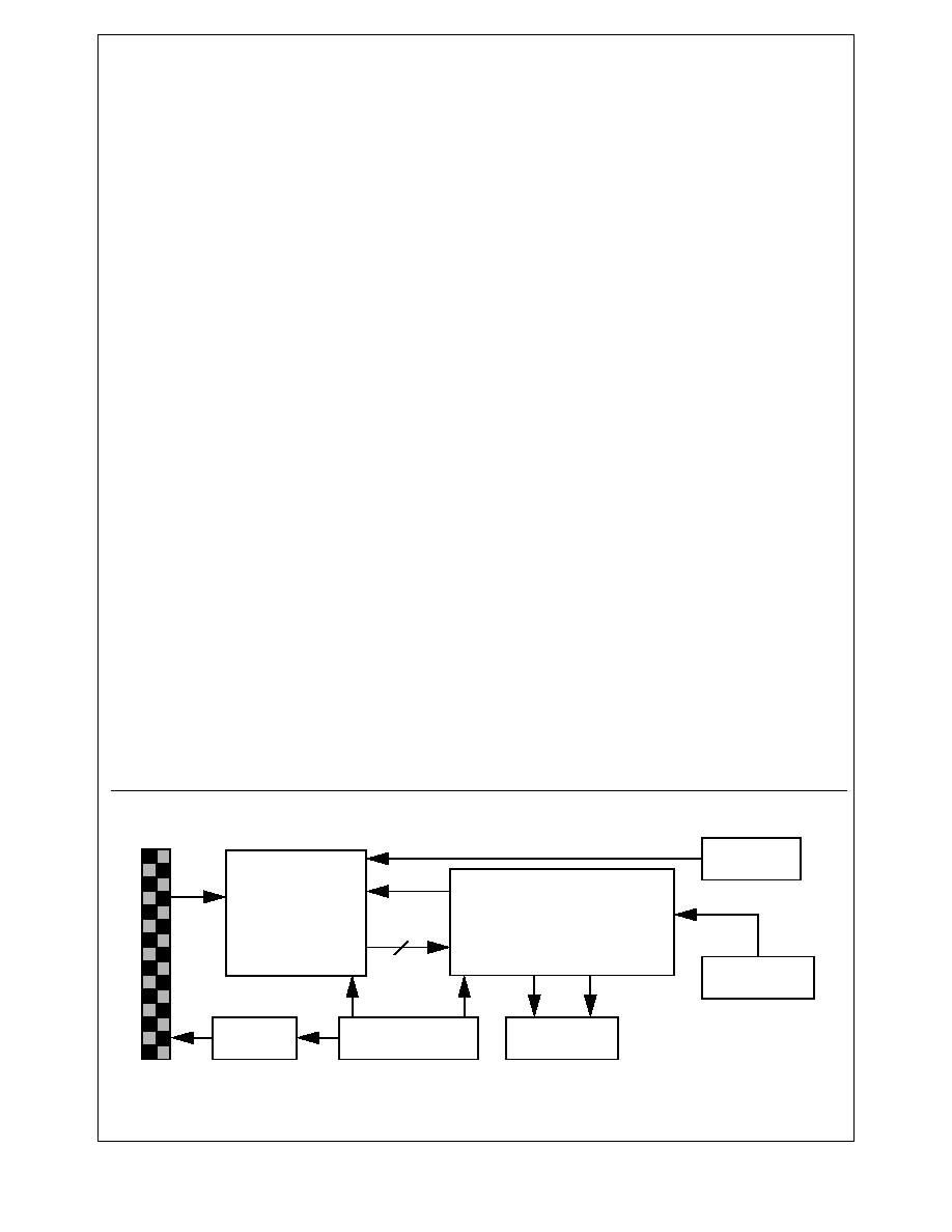
Typical Digital Camera Block Diagram
C
CD/
CIS
S
ens
or
LM98503
Sensor Driver
Timing Generator
Image Processor
Motor Controllers
Microcontroller
10
Auxiliary
Video Input
LM98
503 10-Bi
t, 18 MSPS Camer
a
Si
gnal
P
r
oces
sor
October 2000
www.national.com 2
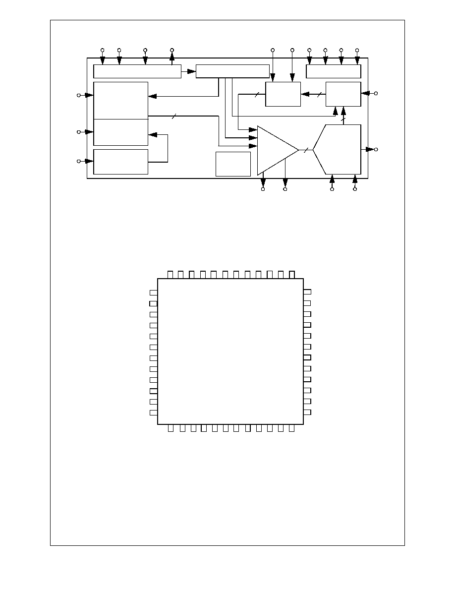
Block Diagram
Figure 1: Chip Block Diagram
1
3
4
5
6
7
8
9
10
12
11
36
34
33
32
31
30
29
28
27
25
26
AUX IN
V IN
AGND
AV+
ACLP
AV+
DGND
DGND
SH
D
DV+
D9
AV
+
DV
+
D8
D7
D6
D5
D1
D2
AG
N
D
AV
+
AO
U
T
+
AO
U
T
-
AG
N
D
AV
+
VREF
T
AG
ND
48 47 46 45 44 43 42 41 40 39
DV+ I/O
VREF
P
VREF
N
VREF
B
DV+ I/O
D0
13 14 15
17
16
18 19 20 21 22
24
37
2
AGND
35
DGND I
/
O
38
D3
23
BL
KCL
P
BOL
LM98503
48 Pin LQFP
RESET
D4
DGND
CLK
SH
P
SI
DA
T
A
SO DA
T
A
DGND I
/
O
SCL
K
/C
E
Pin Out
Figure 2: Pin Out Diagram
Configuration Registers
Timing Control
/CE SCLK
SI DATA
SO DATA
Serial Port Interface
CLK
SHD
SHP
BOL
Correlated
Double
Sampler
Sample/Hold
AUX IN
V IN
ACLP
Analog Clamp
10-Bit
Analog-
to-Digital
Converter
BLKCLP
10-Bit
Data
Output
VREFT
VREFB
Black
Level
Clamp
8
8
2
8
AOUT-
AOUT+
2
Bandgap
Voltage
Reference
VREFN
VREFP
Pixel-Rate
PGA
Pixel-Rate
Offset DAC
LM
98
50
3
www.national.com 3
Ordering Information
43
7
5
21 22
6
AGND
RE
SE
T
AV+
SO D
A
T
A
BL
K
C
L
P
SC
L
K
SI
DA
T
A
D9
D8
D7
D5
D6
D4
D1
D0
ACL
P
35
33
34
32 31 30 29 28
26
D2
D3
44
AV+
16
23
27
47
4,48
AV+
AGND
3
1
V I
N
AU
X I
N
Serial Control Bus
System Control
Digital Video Bus
Camera Control
BOL
15
8
AV+
12
CLK
DV+
DGND
11,39
9,10,38
AOUT+
AOUT-
46
45
/C
E
20
13
SH
P
14
SHD
40
2,41
AV+
AGND
17
VREFP
18
VREFN
DV+ I/O
DGND I/O
25,36
24,37
LM98503
0.1
µ
F
0.1
µ
F
0.1
µ
F
3V
10
µ
F
42
VREFT
19
VREFB
0.1
µ
F
10
µ
F
0.1
µ
F
0.1
µ
F
3V
10
µ
F
1.5K
Typical Application Circuit
Figure 3: Typical Application Circuit Diagram
Commercial
(0°C
T
A
70
70
70
70
°C)
NS Package
LM98503CCVV
LQFP
LM
98
50
3
www.national.com 4
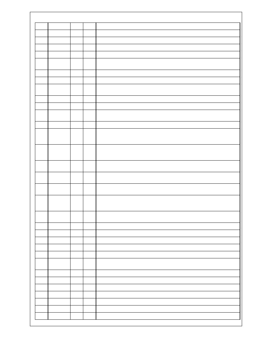
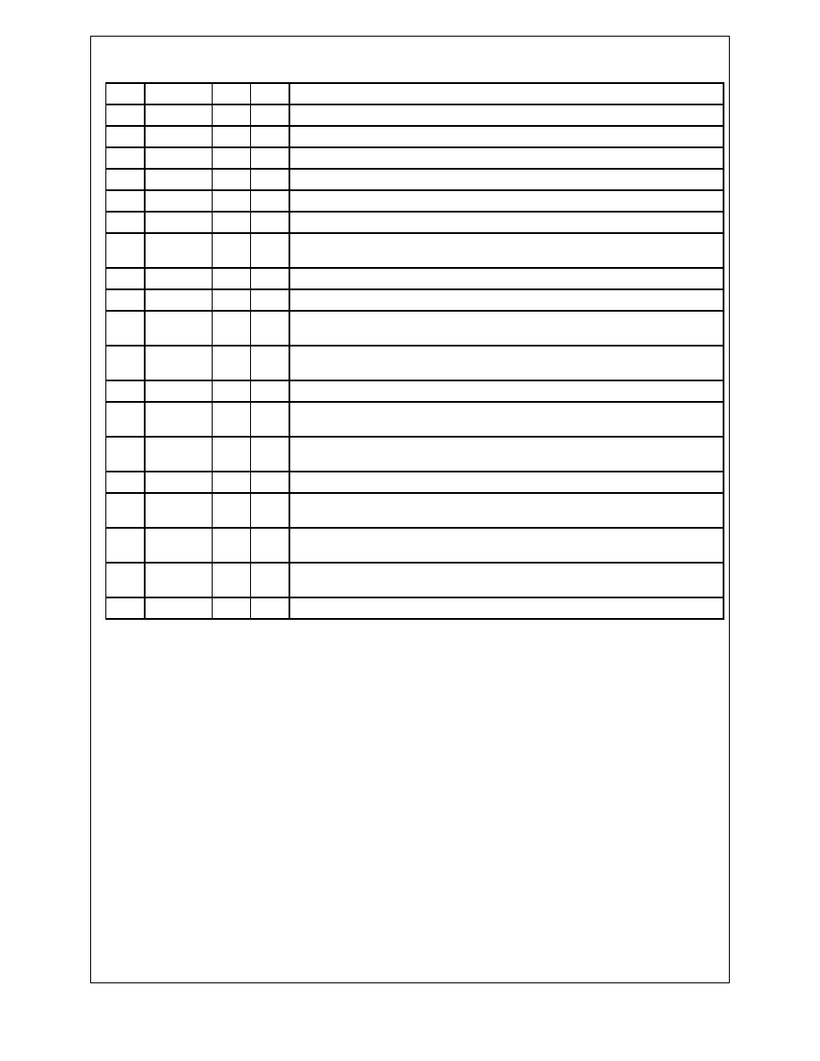
Pin Descriptions
Pin
Name
I/O
Typ
Description
1
AUX IN
I
A
Auxiliary analog input.
2
AGND
P
Analog ground return.
3
V IN
I
A
Analog input. AC-couple input signal through a 0.1
µ
F capacitor.
4
AGND
P
Analog ground return.
5
AV+
P
+3 Volt power supply for the analog circuits. Bypass each supply pin with 0.1
µ
F and
10
µ
F capacitors in parallel.
6
ACLP
I
D
Analog clamp switch.
7
RESET
I
D
Active-high master reset. Float pin when function not being used.
8
AV+
P
+3 Volt power supply for the analog circuits. Bypass each supply pin with 0.1
µ
F and
10
µ
F capacitors in parallel.
9
DGND
P
Digital ground return.
10
DGND
P
Digital ground return.
11
DV+
P
+3 Volt power supply for the digital circuits. Bypass each supply pin with 0.1
µ
F and 10
µ
F
capacitors in parallel.
12
CLK
I
D
18 MHz clock input.
13
SHP
I
D
Correlated double sampler reset voltage clamp override. Programmable active-high or
active-low through serial interface. Connect to +3 Volt digital supply when function not
being used (register values in default condition).
14
SHD
I
D
Correlated double sampler video signal voltage sample override. Programmable active-
high or active-low through serial interface. Connect to +3 Volt digital supply when func-
tion not being used (register values in default condition).
15
BOL
I
D
Active-high beginning of line switch input. Hold high during entire line of effective pixels.
Hold low during blanking period.
16
BLKCLP
I
D
Active-high black level clamp switch input. Pulse high during black pixels to set black
pixel level to the value stored in Output Black Level register. (See page 15.)
17
VREFP
IO
A
Top of DAC reference ladder. Normally bypassed with a 0.1
µ
F capacitor. An external
DAC reference voltage may be applied to this pin.
18
VREFN
IO
A
Bottom of DAC reference ladder. Normally bypassed with a 0.1
µ
F capacitor. An exter-
nal DAC reference voltage may be applied to this pin. Alternately, an external pull-down
resistor may be used to extend the DAC range. (See section 3.0).
19
VREFB
IO
A
Bottom of ADC reference ladder. Normally bypassed with a 0.1
µ
F capacitor and 10
µ
F
capacitors in parallel. An external ADC reference voltage may be applied to this pin.
20
/CE
I
D
Active-low chip enable for the serial interface.
21
SCLK
I
D
Serial interface clock used to decode the serial input data.
22
SI DATA
I
D
Serial interface input port.
23
SO DATA
O
D
Serial interface output port.
24
DGND I/O
P
Digital output driver ground return.
25
DV+ I/O
P
+3 Volt power supply for the digital output driver circuits. Bypass each supply pin with
0.1
µ
F and 10
µ
F capacitors in parallel.
26
D0
O
D
Digital output. Bit 0 of 9 (LSB) of the digital video output bus.
27
D1
O
D
Digital output. Bit 1 of 9 of the digital video output bus.
28
D2
O
D
Digital output. Bit 2 of 9 of the digital video output bus.
29
D3
O
D
Digital output. Bit 3 of 9 of the digital video output bus.
30
D4
O
D
Digital output. Bit 4 of 9 of the digital video output bus.
31
D5
O
D
Digital output. Bit 5 of 9 of the digital video output bus.
32
D6
O
D
Digital output. Bit 6 of 9 of the digital video output bus.
LM
98
50
3
www.national.com 5
Pin Descriptions
(continued)
Legend: (I=Input), (O=Output), (IO=Bi-directional), (P=Power), (D=Digital), (A=Analog)
Pin
Name
I/O
Typ
Description
30
D4
O
D
Digital output. Bit 4 of 9 of the digital video output bus.
31
D5
O
D
Digital output. Bit 5 of 9 of the digital video output bus.
32
D6
O
D
Digital output. Bit 6 of 9 of the digital video output bus.
33
D7
O
D
Digital output. Bit 7 of 9 of the digital video output bus.
34
D8
O
D
Digital output. Bit 8 of 9 of the digital video output bus.
35
D9
O
D
Digital output. Bit 9 of 9 (MSB) of the digital video output bus.
36
DV+ I/O
P
+3 Volt power supply for the digital output driver circuits. Bypass each supply pin with
0.1
µ
F and 10
µ
F capacitors in parallel.
37
DGND I/O
P
Digital output driver ground return.
38
DGND
P
Digital ground return.
39
DV+
P
+3 Volt power supply for the digital circuits. Bypass each supply pin with 0.1
µ
F and 10
µ
F
capacitors in parallel.
40
AV+
P
+3 Volt power supply for the analog circuits. Bypass each supply pin with 0.1
µ
F and
10
µ
F capacitors in parallel.
41
AGND
P
Analog ground return.
42
VREFT
IO
A
Top of ADC reference ladder. Normally bypassed with a 0.1
µ
F capacitor and 10
µ
F
capacitors in parallel. An external ADC reference voltage may be applied to this pin.
43
AV+
P
+3 Volt power supply for the analog circuits. Bypass each supply pin with 0.1
µ
F and
10
µ
F capacitors in parallel.
44
AGND
P
Analog ground return.
45
AOUT-
O
A
Negative differential analog output from correlated double sampler or PGA (selectable
through the serial interface).
46
AOUT+
O
A
Positive differential analog output from correlated double sampler or PGA (selectable
through the serial interface).
47
AV+
P
+3 Volt power supply for the analog circuits. Bypass each supply pin with 0.1
µ
F and
10
µ
F capacitors in parallel.
48
AGND
P
Analog ground return.
LM98503