 | –≠–ª–µ–∫—Ç—Ä–æ–Ω–Ω—ã–π –∫–æ–º–ø–æ–Ω–µ–Ω—Ç: LMC6009 | –°–∫–∞—á–∞—Ç—å:  PDF PDF  ZIP ZIP |

LMC6009
9 Channel Buffer Amplifier for TFT-LCD
General Description
The LMC6009 is a CMOS integrated circuit that buffers 9 ref-
erence voltages for gamma correction in a Thin Film Transis-
tor Liquid Crystal Display (TFT-LCD). Guaranteed to operate
at both 3.3V and 5V supplies, this integrated circuit contains
nine, independent unity gain buffers that can source 130 mA
into a capacitive load without oscillation.
The LMC6009 is useful for buffering gamma voltages into
column drivers that employ the resistor-divider architecture.
High output current capability and fast settling characteristics
of this device improve display quality by minimizing rise time
errors at the outputs of the column driver. The integration of
nine buffers and a multiplexer eliminates the need for dis-
crete buffers and a separate multiplexer (MUX) chip on the
panel.
The LMC6009 is available in 48-pin surface mount TSSOP.
Features
n
Number of inputs
18
n
3.3V and 5V operation
n
Supply current
3.5 mA
n
Settling time
3 µs
n
A/B channel inputs for asymmetrical Gamma
n
Number of outputs
9
n
Number of control inputs
1
n
Built-in thermal shutdown protection
Applications
n
VGA/SVGA TFT-LCD drive circuits
n
Electronic Notebooks
n
Electronic Games
n
Personal Communication Devices
n
Personal Digital Assistants (PDA)
Application in VGA/SVGA TFT-LCD
Ordering Information
Package
Temperature Range
Transport Media
NSC Drawing
48-pin TSSOP
-20∞C≠+75∞C
MTD48
LMC6009MT
LMC6009MTX
Tape and Reel
DS012533-1
May 1999
LMC6009
9
Channel
Buffer
Amplifier
for
TFT-LCD
© 1999 National Semiconductor Corporation
DS012533
www.national.com

Absolute Maximum Ratings
(Note 1)
If Military/Aerospace specified devices are required,
please contact the National Semiconductor Sales Office/
Distributors for availability and specifications.
ESD Tolerance
1.0 kV
Input Voltage
GND≠0.3V
V
+
V
DD
+0.3V
DC
Supply Voltage (V
DD
)
-0.3 to +6.5 V
DC
Operating Temperature
-20∞C to +75∞C
Storage Temperature Range
-55∞C to +150∞C
Maximum Junction Temperature (T
J
)
+150∞C
Maximum Power Dissipation (P
D
)
1.09W
Operating Ratings
(Note 1)
Supply Voltage
2.7V
V
DD
5.5V
Frequency
DC-50 kHz
Thermal Resistance (
JA
)
Derating
8.70 mW/∞C
3V DC Electrical Characteristics
Unless otherwise specified, all limits are guaranteed for T
J
= 25∞C, and V
DD
= 3.0 V
DC
.
Symbol
Parameter
Conditions
Min
Typ
Max
Units
V
DD
Supply Voltage
2.7
3.0
3.3
V
V
OS
Offset Voltage
R
S
= 10k
20
mV
I
B
Input Bias Current
1500
nA
V
OL
Output Voltage, Low
Amp A8 and A9
I
SINK
= 13 mA
GND +
0.2
V
Amp A1≠A7
I
SINK
= 13 mA
GND +
0.6
V
V
OH
Output Voltage, High
Amp A1 and A2
I
SOURCE
= 13 mA
V
DD
≠0.2
V
Amp A3≠A9
I
SOURCE
= 13 mA
V
DD
≠0.6
V
I
SC
Output Short Circuit Current
V
OUT
- 1.65V (Note 1)
80
150
mA
I
DD
Supply Current
No Load
3.5
5
mA
V
L
Load Regulation
V
IN
= 0.3≠3 V
DC
I
SOURCE
= 13 mA
-10
mV
I
SINK
= 13 mA
+10
mV
V
IH
A/B Switch Logic Voltage, High
Select A
2
V
V
IL
A/B Switch Logic Voltage, Low
Select B
0.8
V
I
IH
A/B Switch Logic Current, High
1.5
µA
I
IL
A/B Switch Logic Current, Low
1
µA
A
V
Voltage Gain
0.985
V/V
Note 1: See Test Circuit (
Figure 2 )
5V DC Electrical Characteristics
Unless otherwise specified, all limits are guaranteed for T
J
= 25∞C, and V
DD
= 5 V
DC
.
Symbol
Parameter
Conditions
Min
Typ
Max
Units
V
DD
Supply Voltage
4.5
5
5.5
V
V
OS
Offset Voltage
R
S
= 10k
20
mV
I
B
Input Bias Current
1500
nA
V
OL
Output Voltage, Low
Amp A8 and A9
I
SINK
= 20 mA
GND +
0.2
V
Amp A1≠A7
I
SINK
= 20 mA
GND +
1.0
V
V
OH
Output Voltage, High
Amp A1 and A2
I
SOURCE
= 20 mA
V
DD
≠0.2
V
Amp A3≠A9
I
SOURCE
= 20 mA
V
DD
≠1.0
V
I
SC
Output Short Circuit Current
V
OUT
- 1.65V (Note 1)
120
200
mA
I
DD
Supply Current
No Load
4.5
6
mA
www.national.com
2

5V DC Electrical Characteristics
(Continued)
Unless otherwise specified, all limits are guaranteed for T
J
= 25∞C, and V
DD
= 5 V
DC
.
Symbol
Parameter
Conditions
Min
Typ
Max
Units
V
L
Load Regulation
V
IN
= 0.5≠4.5 V
DC
I
SOURCE
= 20 mA
-10
mV
I
SINK
= 20 mA
+10
mV
V
IH
A/B Switch Logic Voltage, High
Select A
2
V
V
IL
A/B Switch Logic Voltage, Low
Select B
0.8
V
I
IH
A/B Switch Logic Current, High
1.5
µA
I
IL
A/B Switch Logic Current, Low
1
µA
A
V
Voltage Gain
0.985
V/V
AC Electrical Characteristics
Unless otherwise specified, all limits are guaranteed for T
J
= 25∞C, and V
DD
= 3 V
DC
.
Symbol
Parameter
Conditions
Min
Typ
Max
Units
T
S1
Settling Time 1 (Note 2)
I
DC
= 13 mA (Sink/Source)
3
6
µs
T
S2
Settling Time 2 (Note 2)
I
DC
= 13 mA (Sink/Source)
3
6
µs
Note 2: See test circuits (
Figure 3 , Figure 4 and Figure 5 )
DS012533-2
FIGURE 1. Rise and Fall Times at Outputs
www.national.com
3

AC Electrical Characteristics
(Continued)
Description of Pins; LMC6009
Pin 1
NC
Pin 25
NC
Pin 2
NC
Pin 26
NC
Pin 3
NC
Pin 27
NC
Pin 4
A1 in (A)
Pin 28
NC
Pin 5
A1 in (B)
Pin 29
A/B Switch
Pin 6
A2 in (A)
Pin 30
V
DD
(C)
Pin 7
A2 in (B)
Pin 31
GND (C)
Pin 8
A3 in (A)
Pin 32
A9 out
Pin 9
A3 in (B)
Pin 33
A8 out
Pin 10
A4 in (A)
Pin 34
A7 out
Pin 11
A4 in (B)
Pin 35
A6 out
Pin 12
A5 in (A)
Pin 36
A5 out
Pin 13
A5 in (B)
Pin 37
GND (B)
Pin 14
A6 in (A)
Pin 38
V
DD
(B)
Pin 15
A6 in (B)
Pin 39
A4 out
Pin 16
A7 in (A)
Pin 40
A3 out
Pin 17
A7 in (B)
Pin 41
A2 out
Pin 18
A8 in (A)
Pin 42
A1 out
Pin 19
A8 in (B)
Pin 43
GND (A)
Pin 20
A9 in (A)
Pin 44
V
DD
(A)
Pin 21
A9 in (B)
Pin 45
NC
Pin 22
NC
Pin 46
NC
Pin 23
NC
Pin 47
NC
Pin 24
NC
Pin 48
NC
DS012533-3
FIGURE 2.
DS012533-4
FIGURE 3. A1: 13 mA Source only
A2≠A4: 13 mA Sink/Source
DS012533-5
FIGURE 4. 13 mA Sink/Source
DS012533-6
FIGURE 5. A6≠A8: 13 mA Sink/Source
A9: 13 mA Sink Only
www.national.com
4
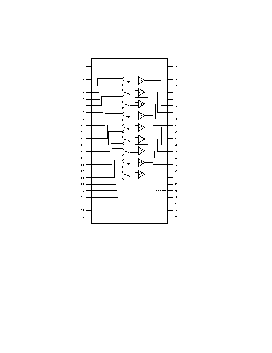
Block Diagram
Applications
The LMC6009 is useful for buffering the nine reference volt-
ages for gamma correction in a TFT-LCD as shown in
Figure 7. The A/B channel inputs allow the user to alternate
two sets of gamma references to compensate for asymmetri-
cal Gamma characteristic during Row Inversion. The
LMC6009 eliminates the need for nine external switches or
an 18-to-9 multiplexer.
Since the buffers in the LMC6009 draw extremely low bias
current (1.5 µA max), large resistance values can be used in
the reference voltage string. This allows the power dissipa-
tion in the gamma reference circuit to be minimized. The
nine buffers are guaranteed to deliver 80 mA to the load, al-
lowing the pixel voltages of the TFT-LCD to settle very
quickly.
DS012533-8
FIGURE 6. Block Diagram of LMC6009
www.national.com
5