
LPC661
Low Power CMOS Operational Amplifier
General Description
The LPC661 CMOS operational amplifier is ideal for opera-
tion from a single supply. It features a wide range of operat-
ing supply voltage from +5V to +15V, rail-to-rail output swing
and an input common-mode range that includes ground.
Performance limitations that have plagued CMOS amplifiers
in the past are not a problem with this design. Input V
OS
,
drift, and broadband noise as well as voltage gain (into 100
k
and 5 k
) are all equal to or better than widely accepted
bipolar equivalents, while the supply current requirement is
typically 55 µA.
This chip is built with National's advanced Double-Poly
Silicon-Gate CMOS process.
See the LPC660 datasheet for a Quad CMOS operational
amplifier or the LPC662 data sheet for a Dual CMOS opera-
tional amplifier with these same features.
Features
(Typical unless otherwise noted)
n
Rail-to-rail output swing
n
Low supply current
55 µA
n
Specified for 100 k
and 5 k
loads
n
High voltage gain
120 dB
n
Low input offset voltage
3 mV
n
Low offset voltage drift
1.3 µV/∞C
n
Ultra low input bias current
2 fA
n
Input common-mode range includes GND
n
Operating range from +5V to +15V
n
Low distortion
0.01% at 1 kHz
n
Slew rate
0.11 V/µs
Applications
n
High-impedance buffer
n
Precision current-to-voltage converter
n
Long-term integrator
n
High-impedance preamplifier
n
Active filter
n
Sample-and-Hold circuit
n
Peak detector
Application Circuits
10 Hz Bandpass Filter
DS011227-21
f
O
= 10 Hz
Q = 2.1
Gain = 18.9 dB
1 Hz Low-Pass Filter
(Maximally Flat, Dual Supply Only)
DS011227-23
August 2000
LPC661
Low
Power
CMOS
Operational
Amplifier
© 2000 National Semiconductor Corporation
DS011227
www.national.com
Absolute Maximum Ratings
(Note 1)
If Military/Aerospace specified devices are required,
please contact the National Semiconductor Sales Office/
Distributors for availability and specifications.
Supply Voltage (V
+
- V
-
)
16V
Differential Input Voltage
±
Supply Voltage
Output Short Circuit to V
+
(Notes 2, 9)
Output Short Circuit to V
-
(Note 2)
Storage Temperature Range
-65∞C to +150∞C
Lead Temperature
(Soldering, 10 sec.)
260∞C
Junction Temperature (Note 3)
150∞C
Power Dissipation
(Note 3)
ESD Rating
(C=100 pF, R=1.5 k
)
1000V
Current at Input Pin
±
5 mA
Current at Output Pin
±
18 mA
Voltage Input/Output Pin
(V
+
) +0.3V, (V
-
) -0.3V
Current at Power Supply Pin
35 mA
Operating Ratings
(Note 1)
Supply Voltage
4.75V
V
+
15.5V
Junction Temperature Range
LPC661AM
-55∞C
T
J
+125∞C
LPC661AI
-40∞C
T
J
+85∞C
LPC661I
-40∞C
T
J
+85∞C
Power Dissipation
(Note 7)
Thermal Resistance (
JA
) (Note 8)
8-Pin DIP
101∞C/W
8-Pin SO
165∞C/W
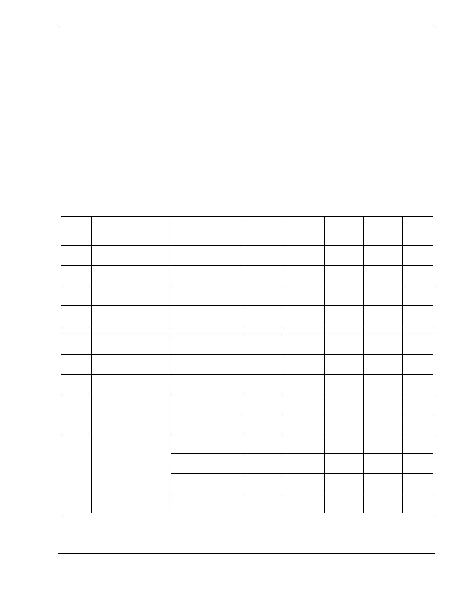
DC Electrical Characteristics
The following specifications apply for V
+
= 5V, V
-
= 0V, V
CM
= 1.5V, V
O
= 2.5V, and R
L
= 1M unless otherwise noted. Bold-
face limits apply at the temperature extremes; all other limits T
J
= 25∞C.
LPC661AM
LPC661AI
LPC661I
Units
(Limit)
Symbol
Parameter
Conditions
Typ
Limit
Limit
Limit
(Note 4)
(Note 4)
(Note 4)
V
OS
Input Offset Voltage
1
3
3
6
mV
3.5
3.3
6.3
TCV
OS
Input Offset Voltage
1.3
µV/∞C
Average Drift
I
B
Input Bias Current
0.002
20
pA
100
4
4
max
I
OS
Input Offset Current
0.001
20
pA
100
2
2
max
R
IN
Input Resistance
>
1
Tera
CMRR
Common Mode
0V
V
CM
12.0V
83
70
70
63
dB
Rejection Ratio
V
+
= 15V
68
68
61
min
+PSRR
Positive Power Supply
5V
V
+
15V
83
70
70
63
dB
Rejection Ratio
68
68
61
min
-PSRR
Negative Power Supply
0V
V
-
-10V
94
84
84
74
dB
Rejection Ratio
82
83
73
min
V
CM
Input Common Mode
V
+
= 5V and 15V
-0.4
-0.1
-0.1
-0.1
V
Voltage Range
for CMRR
50 dB
0
0
0
max
V
+
- 1.9
V
+
- 2.3
V
+
- 2.3
V
+
- 2.3
V
V
+
- 2.6
V
+
- 2.5
V
+
- 2.5
min
A
V
Large Signal
Sourcing
1000
400
400
300
V/mV
Voltage Gain
R
L
= 100 k
(Note 5)
250
300
200
min
Sinking
500
180
180
90
V/mV
R
L
= 100 k
(Note 5)
70
120
70
min
Sourcing
1000
200
200
100
V/mV
R
L
= 5 k
(Note 5)
150
160
80
min
Sinking
250
100
100
50
V/mV
R
L
= 5 k
(Note 5)
35
60
40
min
LPC661
www.national.com
2

DC Electrical Characteristics
(Continued)
The following specifications apply for V
+
= 5V, V
-
= 0V, V
CM
= 1.5V, V
O
= 2.5V, and R
L
= 1M unless otherwise noted. Bold-
face limits apply at the temperature extremes; all other limits T
J
= 25∞C.
LPC661AM
LPC661AI
LPC661I
Units
(Limit)
Symbol
Parameter
Conditions
Typ
Limit
Limit
Limit
(Note 4)
(Note 4)
(Note 4)
V
O
Output Swing
V
+
= 5V
4.987
4.970
4.970
4.940
V
R
L
= 100 k
to 2.5V
4.950
4.950
4.910
min
0.004
0.030
0.030
0.060
V
0.050
0.050
0.090
max
V
+
= 5V
4.940
4.850
4.850
4.750
V
R
L
= 5 k
to 2.5V
4.750
4.750
4.650
min
0.040
0.150
0.150
0.250
V
0.250
0.250
0.350
max
V
+
= 15V
14.970
14.920
14.920
14.880
V
R
L
= 100 k
to 7.5V
14.880
14.880
14.820
min
0.007
0.030
0.030
0.060
V
0.050
0.050
0.090
max
V
+
= 15V
14.840
14.680
14.680
14.580
V
R
L
= 5 k
to 7.5V
14.600
14.600
14.480
min
0.110
0.220
0.220
0.320
V
0.300
0.300
0.400
max
I
O
Output Current
Sourcing, V
O
= 0V
22
16
16
13
mA
V
+
= 5V
12
14
11
min
Sinking, V
O
= 5V
21
16
16
13
mA
12
14
11
min
I
O
Output Current
Sourcing, V
O
= 0V
40
19
28
23
mA
V
+
= 15V
19
25
20
min
Sinking, V
O
= 13V
39
19
28
23
mA
(Note 9)
19
24
19
min
I
S
Supply Current
V
+
= 5V, V
O
= 1.5V
55
60
60
70
µA
70
70
85
max
V
+
= 15V, V
O
= 1.5V
58
75
75
90
µA
85
85
105
max
AC Electrical Characteristics
The following specifications apply for V
+
= 5V, V
-
= 0V, V
CM
= 1.5V, V
O
= 2.5V, and R
L
= 1M unless otherwise noted. Bold-
face limits apply at the temperature extremes; all other limits T
J
= 25∞C.
LPC661AM LPC661AI
LPC661I
Units
(Limit)
Symbol
Parameter
Conditions
Typ
Limit
Limit
Limit
(Note 4)
(Note 4)
(Note 4)
SR
Slew Rate
(Note 6)
0.11
0.07
0.07
0.05
V/µs
0.04
0.05
0.03
min
GBW
Gain-Bandwidth Product
350
kHz
m
Phase Margin
50
Deg
G
M
Gain Margin
17
dB
e
n
Input Referred Voltage Noise
F = 1 kHz
42
nV/
Hz
i
n
Input Referred Current Noise
F = 1 kHz
0.0002
pA/
Hz
T.H.D.
Total Harmonic Distortion
F = 1 kHz, A
V
= -10
0.01
R
L
= 100 k
, V
O
= 8 V
PP
%
V
+
= 15V
LPC661
www.national.com
3

AC Electrical Characteristics
(Continued)
Note 1: Absolute Maximum Ratings indicate limits beyond which damage to the device may occur. Operating Ratings indicate conditions for which the device is in-
tended to be functional, but do not guarantee specific performance limits. For guaranteed specifications and test conditions, see the Electrical Characteristics. The
guaranteed specifications apply only for the test conditions listed.
Note 2: Applies to both single supply and split supply operation. Continuous short circuit operation at elevated ambient temperature can result in exceeding the maxi-
mum allowed junction temperature of 150∞C. Output currents in excess of
±
30 mA over long term may adversely affect reliability.
Note 3: The maximum power dissipation is a function of T
J(max)
,
JA
and T
A
. The maximum allowable power dissipation at any ambient temperature is P
D
=
(T
J(max)
≠T
A
)/
JA
.
Note 4: Limits are guaranteed by testing or correlation.
Note 5: V+ = 15V, V
CM
= 7.5V and R
L
connected to 7.5V. For sourcing tests, 7.5V
V
O
11.5V. For sinking tests, 2.5V
V
O
7.5V.
Note 6: V+ = 15V. Connected as Voltage Follower with 10V step input. Number specified is the slower of the positive and negative slew rates.
Note 7: For operating at elevated temperatures the device must be derated based on the thermal resistance
JA
with P
D
= (T
J
≠T
A
)/
JA
.
Note 8: All numbers apply for packages soldered directly into a PC board.
Note 9: Do not connect output to V
+
when V
+
is greater than 13V or reliability may be adversely affected.
Typical Performance Characteristics
V
S
=
±
7.5V, T
A
= 25∞C unless otherwise specified
Supply Current
vs Supply Voltage
DS011227-26
Input Bias Current
vs Temperature
DS011227-27
Common-Mode Voltage Range
vs Temperature
DS011227-28
Output Characteristics
Current Sinking
DS011227-29
LPC661
www.national.com
4

Typical Performance Characteristics
V
S
=
±
7.5V, T
A
= 25∞C unless otherwise specified (Continued)
Output Characteristics
Current Sourcing
DS011227-30
Input Voltage Noise
vs Frequency
DS011227-31
CMRR vs Frequency
DS011227-32
CMRR vs Temperature
DS011227-33
Power Supply Rejection
Ratio vs Frequency
DS011227-34
Open-Loop Voltage Gain
vs Temperature
DS011227-35
LPC661
www.national.com
5