LMC7215/LMC7225
Micro-Power, Rail-to-Rail CMOS Comparators with
Open-Drain/Push-Pull Outputs and TinyPak
TM
Package
General Description
The LMC7215/LMC7225 are ultra low power comparators
with a maximum of 1 µA power supply current. They are de-
signed to operate over a wide range of supply voltages, from
2V to 8V.
The LMC7215/LMC7225 have a greater than rail-to-rail com-
mon mode voltage range. This is a real advantage in single
supply applications.
The LMC7215 features a push-pull output stage. This fea-
ture allows operation with absolute minimum amount of
power consumption when driving any load.
The LMC7225 features an open drain output. By connecting
an external resistor, the output of the comparator can be
used as a level shifter to any desired voltage to as high as
15V.
The LMC7215/LMC7225 are designed for systems where
low power consumption is the critical parameter.
Guaranteed operation over the full supply voltage range of
2.7V to 5V and rail-to-rail performance makes this compara-
tor ideal for battery-powered applications.
Features
(Typical unless otherwise noted)
n
Ultra low power consumption 0.7 µA
n
Wide range of supply voltages 2V to 8V
n
Input common-mode range beyond V+ and V-
n
Open collector and push-pull output
n
High output current drive: (
@
V
S
= 5V) 45 mA
n
Propagation delay (
@
V
S
= 5V, 10 mV overdrive) 25 µs
n
Tiny SOT23-5 package
n
Latch-up resistance
>
300 mA
Applications
n
Laptop computers
n
Mobile phones
n
Metering systems
n
Hand-held electronics
n
RC timers
n
Alarm and monitoring circuits
n
Window comparators, multivibrators
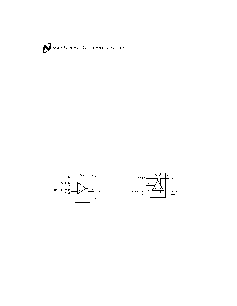
Connection Diagrams
TinyPak
TM
is a trademark of National Semiconductor Corporation.
8≠Pin SO≠8
DS012853-1
Top View
5≠Pin SOT23-5
DS012853-2
Top View
September 1999
LMC7215/LMC7225
Micro-Power
,
Rail-to-Rail
CMOS
Comparators
with
Open-Drain/Push-Pull
Outputs
and
T
inyPak
Package
© 1999 National Semiconductor Corporation
DS012853
www.national.com

Ordering Information
Package
Ordering
NSC Drawing
Package
Supplied As
Information
Number
Marking
5-Pin SOT 23-5
LMC7215IM5
MA05A
C02B
1k Tape and Reel
5-Pin SOT 23-5
LMC7225IM5
MA05A
C03B
1k Tape and Reel
5-Pin SOT 23-5
LMC7215IM5X
MA05A
C02B
3k Tape and Reel
5-Pin SOT 23-5
LMC7225IM5X
MA05A
C03B
3k Tape and Reel
8-Pin SO-8
LMC7215IM
M08A
LMC7215IM
Rails
8-Pin SO-8
LMC7225IM
M08A
LMC7225IM
Rails
8-Pin SO-8
LMC7215IMX
M08A
LMC7215IM
2.5k Tape and Reel
8-Pin SO-8
LMC7225IMX
M08A
LMC7225IM
2.5k Tape and Reel
www.national.com
2

Absolute Maximum Ratings
(Note 1)
If Military/Aerospace specified devices are required,
please contact the National Semiconductor Sales Office/
Distributors for availability and specifications.
ESD Tolerance (Note 2)
2 kV
Differential Input Voltage
(V
CC
)+0.3V to (-V
CC
)-0.3V
Voltage at Input/Output Pin
(V
CC
)+0.3V to (-V
CC
)-0.3V
Supply Voltage (V
+
≠V
-
)
10V
Current at Input Pin
±
5 mA
Current at Output Pin (Note 3)
±
30 mA
Current at Power Supply Pin
40 mA
Lead Temperature
(soldering, 10 sec)
260∞C
Storage Temperature Range
-65∞C to +150∞C
Junction Temperature (Note 4)
150∞C
Operating Ratings
(Note 1)
Supply Voltage
2V
V
CC
8V
Junction Temperature Range
LMC7215IM, LMC7225IM
-40∞C
T
J
+85∞C
Thermal Resistance (
JA
)
M Package, 8-Pin Surface Mount
165∞C/W
SOT23-5 Package
325∞C/W
2.7V to 5V Electrical Characteristics
Unless otherwise specified, all limits guaranteed for T
J
= 25∞C, V
+
= 2.7V to 5V, V
-
= 0V, V
CM
= V
O
= V+/2. Boldface limits
apply at the temperature extremes.
Typ
LMC7215
LMC7225
Symbol
Parameter
Conditions
(Note 5)
Limit
Limit
Units
(Note 6)
(Note 6)
V
OS
Input Offset Voltage
1
6
6
mV
8
8
max
TCV
OS
Input Offset Voltage
2
µV/∞C
Average Drift
I
B
Input Current
5
fA
I
OS
Input Offset Current
1
fA
CMRR
Common Mode
(Note 7)
80
60
60
dB
Rejection Ratio
min
PSRR
Power Supply
V
+
= 2.2V to 8V
90
60
60
dB
Rejection Ratio
min
A
V
Voltage Gain
140
dB
CMVR
Input Common-Mode
V
+
= 2.7V
3.0
2.9
2.9
V
Voltage Range
CMRR
>
50 dB
2.7
2.7
min
V
+
= 2.7V
-0.2
0.0
0.0
V
CMRR
>
50 dB
0.2
0.2
max
V
+
= 5.0V
5.3
5.2
5.2
V
CMRR
>
50 dB
5.0
5.0
min
V
+
= 5.0V
-0.3
-0.2
-0.2
V
CMRR
>
50 dB
0.0
0.0
max
V
OH
Output Voltage High
V
+
= 2.2V
2.05
1.8
NA
V
I
OH
= 1.5 mA
1.7
min
V
+
= 2.7V
2.05
2.3
NA
V
I
OH
= 2.0 mA
2.2
min
V
+
= 5.0V
4.8
4.6
NA
V
I
OH
= 4.0 mA
4.5
min
V
OL
Output Voltage Low
V
+
= 2.2V
0.17
0.4
0.4
V
I
OH
= 1.5 mA
0.5
0.5
max
V
+
= 2.7V
0.17
0.4
0.4
V
I
OH
= 2.0 mA
0.5
0.5
max
V
+
= 5.0V
0.2
0.4
0.4
V
I
OH
= 4.0 mA
0.5
0.5
max
I
SC+
Output Short Circuit
V
+
= 2.7V, Sourcing
15
NA
mA
Current (Note 10)
V
+
= 5.0V, Sourcing
50
NA
mA
I
SC-
Output Short Circuit
V
+
= 2.7V, Sinking
12
mA
www.national.com
3

2.7V to 5V Electrical Characteristics
(Continued)
Unless otherwise specified, all limits guaranteed for T
J
= 25∞C, V
+
= 2.7V to 5V, V
-
= 0V, V
CM
= V
O
= V+/2. Boldface limits
apply at the temperature extremes.
Typ
LMC7215
LMC7225
Symbol
Parameter
Conditions
(Note 5)
Limit
Limit
Units
(Note 6)
(Note 6)
Current (Note 10)
V
+
= 5.0V, Sinking
30
mA
I
Leakage
Output Leakage Current
V
+
= 2.2V
nA
V
IN
+ = 0.1V, V
IN
- = 0V,
0.01
NA
500
max
V
OUT
= 15V
I
S
Supply Current
V
+
= 5.0V
0.7
1
1
µA
V
IN
+ = 5V, V
IN
- = 0V
1.2
1.2
max
AC Electrical Characteristics
Unless otherwise specified, T
J
= 25∞C, V
+
= 5V, V
-
= 0V, V
CM
= V
+
/2
LMC7215
LMC7225
Symbol
Parameter
Conditions
Typ
Typ
Units
(Note 5)
(Notes 5, 8)
t
rise
Rise Time
Overdrive = 10 mV (Note 8)
1
12.2
µs
t
fall
Fall Time
Overdrive = 10 mV (Note 8)
0.4
0.35
µs
t
PHL
Propagation Delay
(Notes 8, 9)
Overdrive = 10 mV
24
24
µs
(High to Low)
Overdrive = 100 mV
12
12
V
+
= 2.7V
Overdrive = 10 mV
17
17
µs
(Notes 8, 9)
Overdrive = 100 mV
11
11
t
PLH
Propagation Delay
(Notes 8, 9)
Overdrive = 10 mV
24
29
µs
(Low to High)
Overdrive = 100 mV
12
17
V
+
= 2.7V
Overdrive = 10 mV
17
22
µs
(Notes 8, 9)
Overdrive = 100 mV
11
16
Note 1: Absolute Maximum Ratings indicate limits beyond which damage to the device may occur. Operating Ratings indicate conditions for which the device is in-
tended to be functional, but specific performance is not guaranteed. For guaranteed specifications and the test conditions, see the Electrical Characteristics.
Note 2: Human body model, 1.5 k
in series with 100 pF.
Note 3: Applies to both single-supply and split-supply operation. Continuous short circuit operation at elevated ambient temperature can result in exceeding the
maximum allowed junction temperature of 150∞C.
Note 4: The maximum power dissipation is a function of T
J(max)
,
JA
, and T
A
. The maximum allowable power dissipation at any ambient temperature is
P
D
= (T
J(max)
- T
A
)/
JA
. All numbers apply for packages soldered directly into a PC board.
Note 5: Typical values represent the most likely parametric norm.
Note 6: All limits are guaranteed by testing or statistical analysis.
Note 7: CMRR measured at V
CM
= 0V to 2.5V and 2.5V to 5V when V
S
= 5V, V
CM
= 0.2V to 1.35V and 1.35V to 2.7V when V
S
= 2.7V. This eliminates units that
have large V
OS
at the V
CM
extremes and low or opposite V
OS
at V
CM
= V
S
/2.
Note 8: All measurements made at 10 kHz. A 100 k
pull-up resistor was used when measuring the LMC7225. C
LOAD
= 50 pF including the test jig and scope probe.
The rise times of the LMC7225 are a function of the R-C time constant.
Note 9: Input step voltage for the propagation measurements is 100 mV.
Note 10: Do not short the output of the LMC7225 to voltages greater than 10V or damage may occur.
www.national.com
4
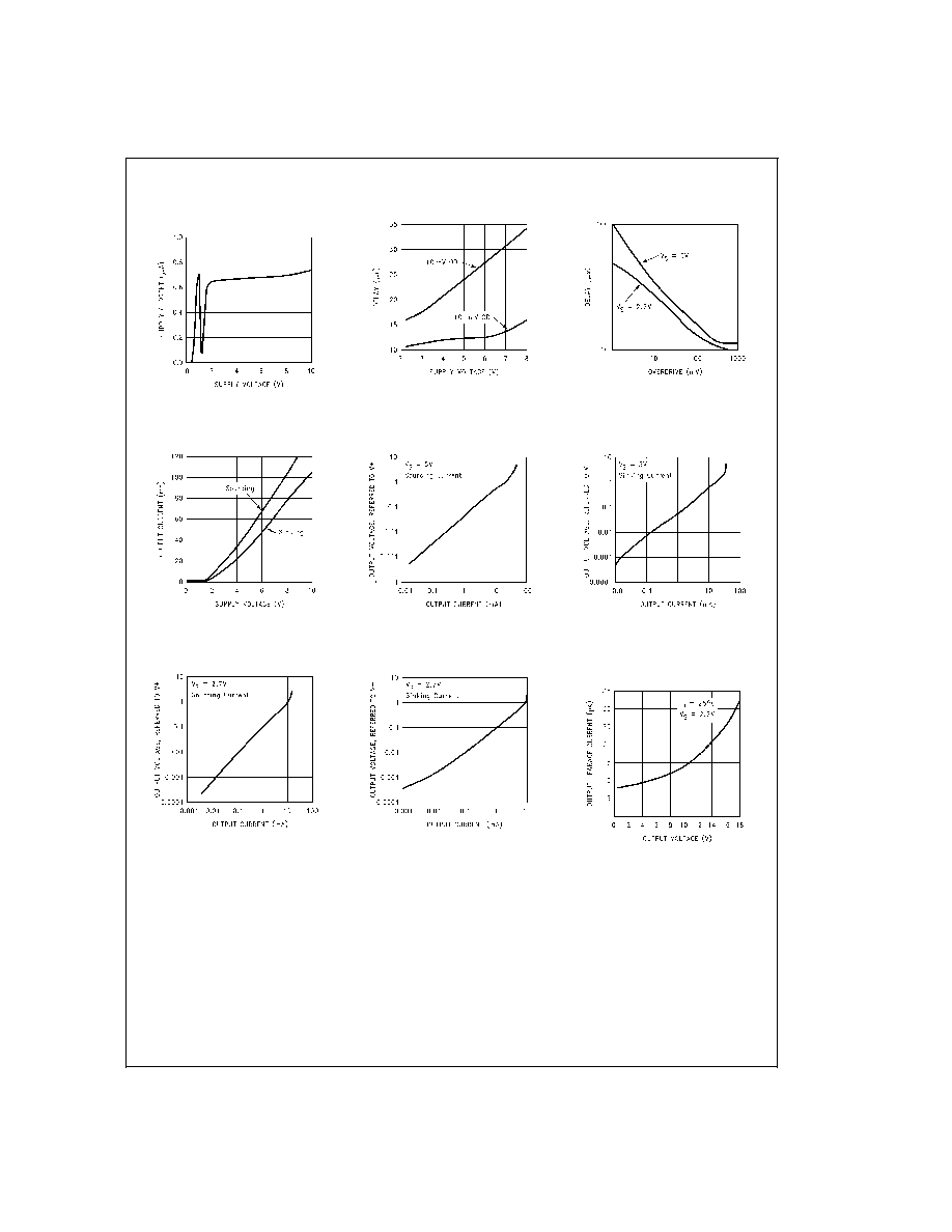
Typical Performance Characteristics
T
A
= 25∞C unless otherwise specified
Supply Current vs
Supply Voltage
DS012853-3
Prop Delay vs V
Supply
DS012853-12
Prop Delay vs Overdrive
DS012853-13
Short Circuit Current vs
V
Supply
DS012853-14
Output Voltage vs Output
Current LMC7215
DS012853-15
Output Voltage vs
Output Current
DS012853-16
Output Voltage vs
Output Current LMC7215
DS012853-17
Output Voltage vs
Output Current
DS012853-18
Output Leakage Current
vs Output Voltage
LMC7225
DS012853-19
www.national.com
5