
LMF100
High Performance Dual Switched Capacitor Filter
General Description
The LMF100 consists of two independent general purpose
high performance switched capacitor filters. With an external
clock and 2 to 4 resistors, various second-order and
first-order filtering functions can be realized by each filter
block. Each block has 3 outputs. One output can be config-
ured to perform either an allpass, highpass, or notch func-
tion. The other two outputs perform bandpass and lowpass
functions. The center frequency of each filter stage is tuned
by using an external clock or a combination of a clock and re-
sistor ratio. Up to a 4th-order biquadratic function can be re-
alized with a single LMF100. Higher order filters are imple-
mented by simply cascading additional packages, and all the
classical filters (such as Butterworth, Bessel, Elliptic, and
Chebyshev) can be realized.
The LMF100 is fabricated on National Semiconductor's high
performance
analog
silicon
gate
CMOS
process,
LMCMOS
TM
. This allows for the production of a very low off-
set, high frequency filter building block. The LMF100 is
pin-compatible with the industry standard MF10, but pro-
vides greatly improved performance.
Features
n
Wide 4V to 15V power supply range
n
Operation up to 100 kHz
n
Low offset voltage:
typically
(50:1 or 100:1 mode):
Vos1 =
�
5 mV
Vos2 =
�
15 mV
Vos3 =
�
15 mV
n
Low crosstalk -60 dB
n
Clock to center frequency ratio accuracy
�
0.2% typical
n
f
0
x Q range up to 1.8 MHz
n
Pin-compatible with MF10
4th Order 100 kHz Butterworth Lowpass Filter
Connection Diagram
LMCMOS
TM
is a trademark of National Semiconductor Corporation.
DS005645-2
DS005645-3
Surface Mount and Dual-In-Line Package
DS005645-18
Top View
Order Number
LMF100CCN or LMF100CIWM
See NS Package Number N20A or M20B
July 1999
LMF100
High
Performance
Dual
Switched
Capacitor
Filter
� 1999 National Semiconductor Corporation
DS005645
www.national.com
Absolute Maximum Ratings
(Note 1)
If Military/Aerospace specified devices are required,
please contact the National Semiconductor Sales Office/
Distributors for availability and specifications.
(Note 14)
Supply Voltage (V
+
- V
-
)
16V
Voltage at Any Pin
V
+
+ 0.3V
V
-
- 0.3V
Input Current at Any Pin (Note 2)
5 mA
Package Input Current (Note 2)
20 mA
Power Dissipation (Note 3)
500 mW
Storage Temperature
150�C
ESD Susceptability (Note 11)
2000V
Soldering Information
N Package: 10 sec.
260�C
J Package: 10 sec.
300�C
SO Package:
Vapor Phase (60 sec.)
215�C
Infrared (15 sec.)
220�C
See AN-450 "Surface Mounting Methods and Their Effect
on Product Reliability" (Appendix D) for other methods of
soldering surface mount devices.
Operating Ratings
(Note 1)
Temperature Range
T
MIN
T
A
T
MAX
LMF100CCN
0�C
T
A
+70�C
LMF100CIWM
-40�C
T
A
+85�C
Supply Voltage
4V
V
+
- V
-
15V
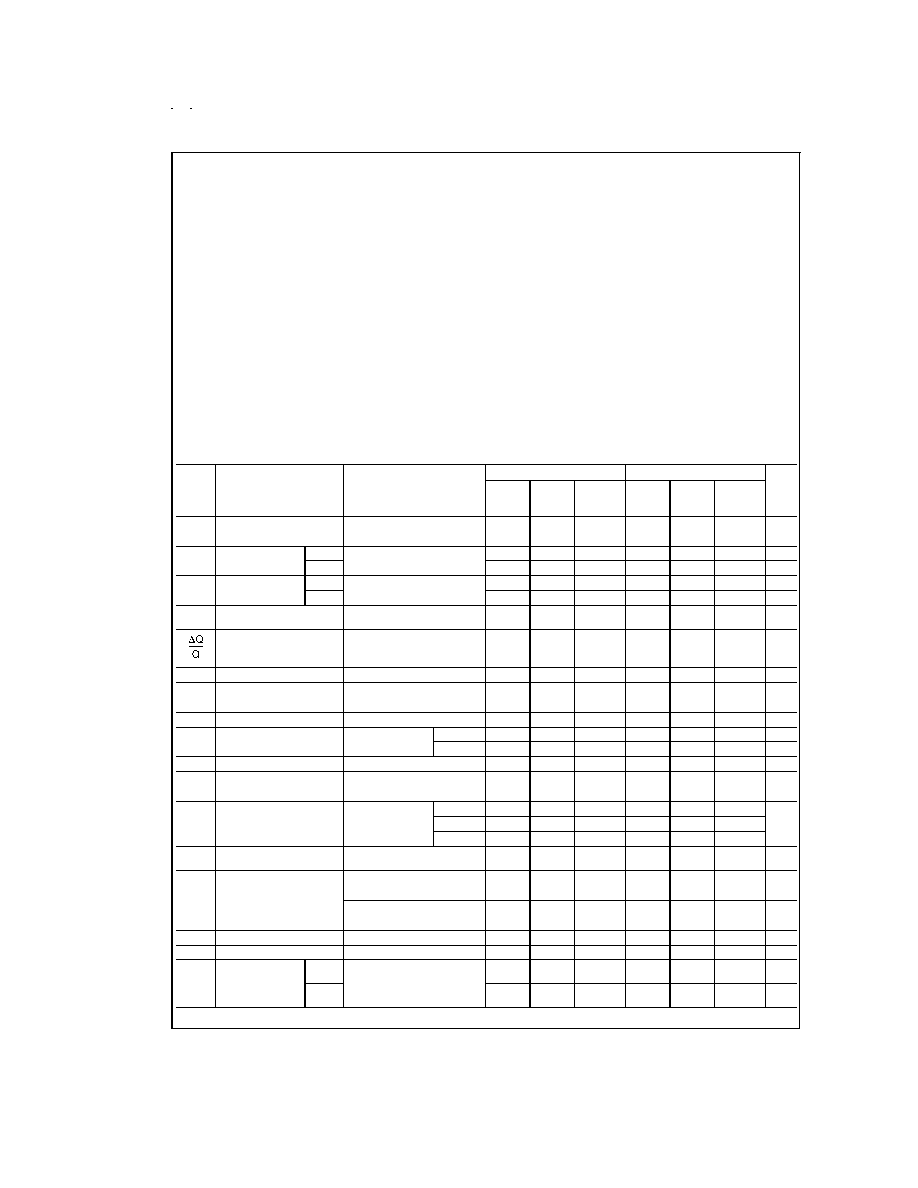
Electrical Characteristics
The following specifications apply for Mode 1, Q = 10 (R
1
= R
3
= 100k, R
2
= 10k), V
+
= +5V and V
-
= -5V unless otherwise
specified. Boldface limits apply for T
MIN
to T
MAX
; all other limits T
A
= T
J
= 25�C.
Symbol
Parameter
Conditions
LMF100CCN
LMF100CIWM
Units
Typical
(Note 8)
Tested
Limit
(Note 9)
Design
Limit
(Note 10)
Typical
(Note 8)
Tested
Limit
(Note 9)
Design
Limit
(Note 10)
I
s
Maximum Supply Current
f
CLK
= 250 kHz
9
13
13
9
13
mA
No Input Signal
f
0
Center Frequency
MIN
0.1
0.1
Hz
Range
MAX
100
100
kHz
f
CLK
Clock Frequency
MIN
5.0
5.0
Hz
Range
MAX
3.5
3.5
MHz
f
CLK
/f
0
Clock to Center Frequency
Ratio Deviation
V
Pin12
= 5V or 0V
f
CLK
= 1 MHz
�
0.2
�
0.8
�
0.8
�
0.2
�
0.8
%
Q Error (MAX) (Note 4)
Q = 10, Mode 1
V
Pin12
= 5V or 0V
f
CLK
= 1 MHz
�
0.5
�
5
�
6
�
0.5
�
6
%
H
OBP
Bandpass Gain at f
0
f
CLK
= 1 MHz
0
�
0.4
�
0.4
0
�
0.4
dB
H
OLP
DC Lowpass Gain
R
1
= R
2
= 10k
0
�
0.2
�
0.2
0
�
0.2
dB
f
CLK
= 250 kHz
V
OS1
DC Offset Voltage (Note 5)
f
CLK
= 250 kHz
�
5.0
�
15
�
15
�
5.0
�
15
mV
V
OS2
DC Offset Voltage (Note 5)
f
CLK
= 250 kHz
S
A/B
= V
+
�
30
�
80
�
80
�
30
�
80
mV
S
A/B
= V
-
�
15
�
70
�
70
�
15
�
70
mV
V
OS3
DC Offset Voltage (Note 5)
f
CLK
= 250 kHz
�
15
�
40
�
60
�
15
�
60
mV
Crosstalk (Note 6)
A Side to B Side or
-60
-60
dB
B Side to A Side
Output Noise (Note 12)
f
CLK
= 250 kHz
N
40
40
20 kHz Bandwidth
BP
320
320
�V
100:1 Mode
LP
300
300
Clock Feedthrough
(Note 13)
f
CLK
= 250 kHz 100:1 Mode
6
6
mV
V
OUT
Minimum Output
R
L
= 5k
+4.0
�
3.8
�
3.7
+4.0
�
3.7
V
Voltage Swing
(All Outputs)
-4.7
-4.7
R
L
= 3.5k
+3.9
+3.9
V
(All Outputs)
-4.6
-4.6
GBW
Op Amp Gain BW Product
5
5
MHz
SR
Op Amp Slew Rate
20
20
V/�s
I
sc
Maximum Output
Short
Source
(All Outputs)
12
12
mA
Circuit Current
(Note 7)
Sink
45
45
mA
www.national.com
2

Electrical Characteristics
(Continued)
The following specifications apply for Mode 1, Q = 10 (R
1
= R
3
= 100k, R
2
= 10k), V
+
= +5V and V
-
= -5V unless otherwise
specified. Boldface limits apply for T
MIN
to T
MAX
; all other limits T
A
= T
J
= 25�C.
Symbol
Parameter
Conditions
LMF100CCN
LMF100CIWM
Units
Typical
(Note 8)
Tested
Limit
(Note 9)
Design
Limit
(Note 10)
Typical
(Note 8)
Tested
Limit
(Note 9)
Design
Limit
(Note 10)
I
IN
Input Current on Pins: 4, 5,
10
10
�A
6, 9, 10, 11, 12, 16, 17
Electrical Characteristics
The following specifications apply for Mode 1, Q = 10 (R
1
= R
3
= 100k, R
2
= 10k), V
+
= +2.50V and V
-
= -2.50V unless oth-
erwise specified. Boldface limits apply for T
MIN
to T
MAX
; all other limits T
A
= T
J
= 25�C.
Symbol
Parameter
Conditions
LMF100CCN
LMF100CIWM
Units
Typical
(Note 8)
Tested
Limit
(Note 9)
Design
Limit
(Note
10)
Typical
(Note 8)
Tested
Limit
(Note 9)
Design
Limit
(Note
10)
I
s
Maximum Supply
Current
f
CLK
= 250 kHz
No Input Signal
8
12
12
8
12
mA
f
0
Center Frequency
MIN
0.1
0.1
Hz
Range
MAX
50
50
kHz
f
CLK
Clock Frequency
MIN
5.0
5.0
Hz
Range
MAX
1.5
1.5
MHz
f
CLK
/f
0
Clock to Center
V
Pin12
= 2.5V or 0V
�
0.2
�
1
�
1
�
0.2
�
1
%
Frequency Ratio Deviation
f
CLK
= 1 MHz
Q Error (MAX)
Q = 10, Mode 1
(Note 4)
V
Pin12
= 5V or 0V
�
0.5
�
5
�
8
�
0.5
�
8
%
f
CLK
= 1 MHz
H
OBP
Bandpass Gain at f
0
f
CLK
= 1 MHz
0
�
0.4
�
0.5
0
�
0.5
dB
H
OLP
DC Lowpass Gain
R
1
= R
2
= 10k
0
�
0.2
�
0.2
0
�
0.2
dB
f
CLK
= 250 kHz
V
OS1
DC Offset Voltage (Note 5)
f
CLK
= 250 kHz
�
5.0
�
15
�
15
�
5.0
�
15
mV
V
OS2
DC Offset Voltage (Note 5)
f
CLK
= 250 kHz
S
A/B
= V
+
�
20
�
60
�
60
�
20
�
60
mV
S
A/B
= V
-
�
10
�
50
�
60
�
10
�
60
mV
V
OS3
DC Offset Voltage (Note 5)
f
CLK
= 250 kHz
�
10
�
25
�
30
�
10
�
30
mV
Crosstalk (Note 6)
A Side to B Side or
-65
-65
dB
B Side to A Side
Output Noise (Note 12)
f
CLK
= 250 kHz
N
25
25
20 kHz Bandwidth
BP
250
250
�V
100:1 Mode
LP
220
220
Clock Feedthrough (Note 13)
f
CLK
= 250 kHz 100:1 Mode
2
2
mV
V
OUT
Minimum Output
R
L
= 5k
+1.6
�
1.5
�
1.4
+1.6
�
1.4
V
Voltage Swing
(All Outputs)
-2.2
-2.2
R
L
= 3.5k
+1.5
+1.5
V
(All outputs)
-2.1
-2.1
GBW
Op Amp Gain BW Product
5
5
MHz
SR
Op Amp Slew Rate
18
18
V/�s
I
sc
Maximum Output
Short Circuit
Source
(All Outputs)
10
10
mA
Current (Note 7)
Sink
20
20
mA
www.national.com
3
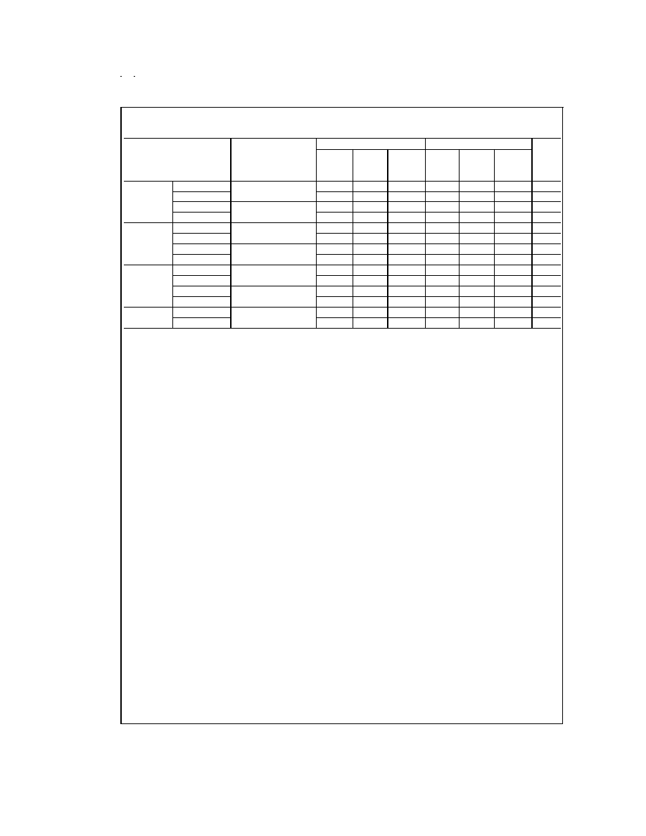
Logic Input Characteristics
Boldface limits apply for T
MIN
to T
MAX
; all other limits T
A
= T
J
= 25�C.
Parameter
Conditions
LMF100CCN
LMF100CIWM
Units
Typical
Tested
Design
Typical
Tested
Design
(Note 8)
Limit
Limit
(Note 8)
Limit
Limit
(Note 9)
(Note 10)
(Note 9)
(Note 10)
CMOS Clock
MIN Logical "1"
V
+
= +5V, V
-
= -5V,
+3.0
+3.0
+3.0
V
Input Voltage
MAX Logical "0"
V
LSh
= 0V
-3.0
-3.0
-3.0
V
MIN Logical "1"
V
+
= +10V, V
-
= 0V,
+8.0
+8.0
+8.0
V
MAX Logical "0"
V
LSh
= +5V
+2.0
+2.0
+2.0
V
TTL Clock
MIN Logical "1"
V
+
= +5V, V
-
= -5V,
+2.0
+2.0
+2.0
V
Input Voltage
MAX Logical "0"
V
LSh
= 0V
+0.8
+0.8
+0.8
V
MIN Logical "1"
V
+
= +10V, V
-
= 0V,
+2.0
+2.0
+2.0
V
MAX Logical "0"
V
LSh
= 0V
+0.8
+0.8
+0.8
V
CMOS Clock
MIN Logical "1"
V
+
= +2.5V, V
-
= -2.5V,
+1.5
+1.5
+1.5
V
Input Voltage
MAX Logical "0"
V
LSh
= 0V
-1.5
-1.5
-1.5
V
MIN Logical "1"
V
+
= +5V, V
-
= 0V,
+4.0
+4.0
+4.0
V
MAX Logical "0"
V
LSh
= +2.5V
+1.0
+1.0
+1.0
V
TTL Clock
MIN Logical "1"
V
+
= +5V, V
-
= 0V,
+2.0
+2.0
+2.0
V
Input Voltage
MAX Logical "0"
V
LSh
= 0V, V
D
+
= 0V
+0.8
+0.8
+0.8
V
Note 1: Absolute Maximum Ratings indicate limits beyond which damage to the device may occur. Operating Ratings indicate conditions for which the device is in-
tended to be functional. These ratings do not guarantee specific performance limits, however. For guaranteed specifications and test conditions, see the Electrical
Characteristics. The guaranteed specifications apply only for the test conditions listed. Some performance characteristics may degrade when the device is not op-
erated under the listed test conditions.
Note 2: When the input voltage (V
IN
) at any pin exceeds the power supply rails (V
IN
<
V
-
or V
IN
>
V
+
) the absolute value of current at that pin should be limited
to 5 mA or less. The sum of the currents at all pins that are driven beyond the power supply voltages should not exceed 20 mA.
Note 3: The maximum power dissipation must be derated at elevated temperatures and is dictated by T
JMAX
,
JA
, and the ambient temperature, T
A
. The maximum
allowable power dissipation at any temperature is P
D
= (T
JMAX
- T
A
)/
JA
or the number given in the Absolute Maximum Ratings, whichever is lower. For this device,
T
JMAX
= 125�C, and the typical junction-to-ambient thermal resistance of the LMF100CIN when board mounted is 55�C/W. For the LMF100CIWM this number is
66�C/W.
Note 4: The accuracy of the Q value is a function of the center frequency (f
0
). This is illustrated in the curves under the heading "Typical Peformance Characteristics".
Note 5: V
os1
, V
os2
, and V
os3
refer to the internal offsets as discussed in the Applications Information section 3.4.
Note 6: Crosstalk between the internal filter sections is measured by applying a 1 V
RMS
10 kHz signal to one bandpass filter section input and grounding the input
of the other bandpass filter section. The crosstalk is the ratio between the output of the grounded filter section and the 1 V
RMS
input signal of the other section.
Note 7: The short circuit source current is measured by forcing the output that is being tested to its maximum positive voltage swing and then shorting that output
to the negative supply. The short circuit sink current is measured by forcing the output that is being tested to its maximum negative voltage swing and then shorting
that output to the positive supply. These are the worst case conditions.
Note 8: Typicals are at 25�C and represent most likely parametric norm.
Note 9: Tested limits are guaranteed to National's AOQL (Average Outgoing Quality Level).
Note 10: Design limits are guaranteed to National's AOQL (Average Outgoing Quality Level) but are not 100% tested.
Note 11: Human body model, 100 pF discharged through a 1.5 k
resistor.
Note 12: In 50:1 mode the output noise is 3 dB higher.
Note 13: In 50:1 mode the clock feedthrough is 6 dB higher.
Note 14: A military RETS specification is available upon request.
www.national.com
4
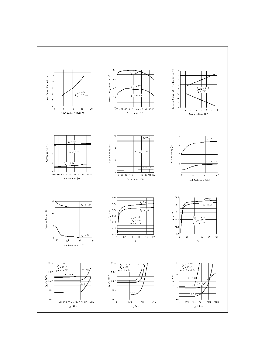
Typical Performance Characteristics
Power Supply Current vs
Power Supply Voltage
DS005645-40
Power Supply Current vs
Temperature
DS005645-41
Output Swing vs
Supply Voltage
DS005645-42
Positive Output Swing
vs Temperature
DS005645-43
Negative Output Swing
vs Temperature
DS005645-44
Positive Output Voltage
Swing vs Load Resistance
DS005645-45
Negative Output Voltage
Swing vs Load Resistance
DS005645-46
f
CLK
/f
0
Ratio vs Q
DS005645-47
f
CLK
/f
0
Ratio vs Q
DS005645-48
f
CLK
/f
0
Ratio vs f
CLK
DS005645-49
f
CLK
/f
0
Ratio vs f
CLK
DS005645-50
f
CLK
/f
0
Ratio vs f
CLK
DS005645-51
www.national.com
5