 | –≠–ª–µ–∫—Ç—Ä–æ–Ω–Ω—ã–π –∫–æ–º–ø–æ–Ω–µ–Ω—Ç: LMH6321TS | –°–∫–∞—á–∞—Ç—å:  PDF PDF  ZIP ZIP |

LMH6321
300 mA High Speed Buffer with Adjustable Current Limit
General Description
The LMH6321 is a high speed unity gain buffer that slews at
1800 V/µs and has a small signal bandwidth of 110 MHz
while driving a 50
load. It can drive
±
300 mA continuously
and will not oscillate while driving large capacitive loads.
The LMH6231 features an adjustable current limit. The cur-
rent limit is continuously adjustable from 10 mA to 300 ma
with a
±
5 mA
±
5% accuracy. The current limit is set by
adjusting an external reference current with a resistor. The
current can be easily and instantly adjusted, as needed by
connecting the resistor to a DAC to form the reference
current. The sourcing and sinking currents share the same
current limit.
The LMH6321 is available in a space saving 8-pin PSOP or
a 7-pin TO-263 power package. The PSOP package fea-
tures an exposed pad on the bottom of the package to
increase its heat sinking capability. The LMH6321 can be
used within the feedback loop of an operational amplifier to
boost the current output or as a stand alone buffer.
Features
n
High slew rate
1800 V/µs
n
Wide bandwidth
110 MHz
n
Continuous output current
±
300 mA
n
Output current limit tolerance
±
5 mA
±
5%
n
Wide supply voltage range
5V to
±
15V
n
Wide temperature range
-40∞C to +125∞C
n
Adjustable current limit
n
High capacitive load drive
n
Thermal shutdown error flag
Applications
n
Line driver
n
Pin driver
n
Sonar driver
n
Motor control
Connection Diagrams
8-Pin PSOP
7-Pin TO-263
20138625
20138626
Note: V
-
pin is connected to tab on back of each package
April 2006
LMH6321
300
mA
High
Speed
Buffer
with
Adjustable
Current
Limit
© 2006 National Semiconductor Corporation
DS201386
www.national.com
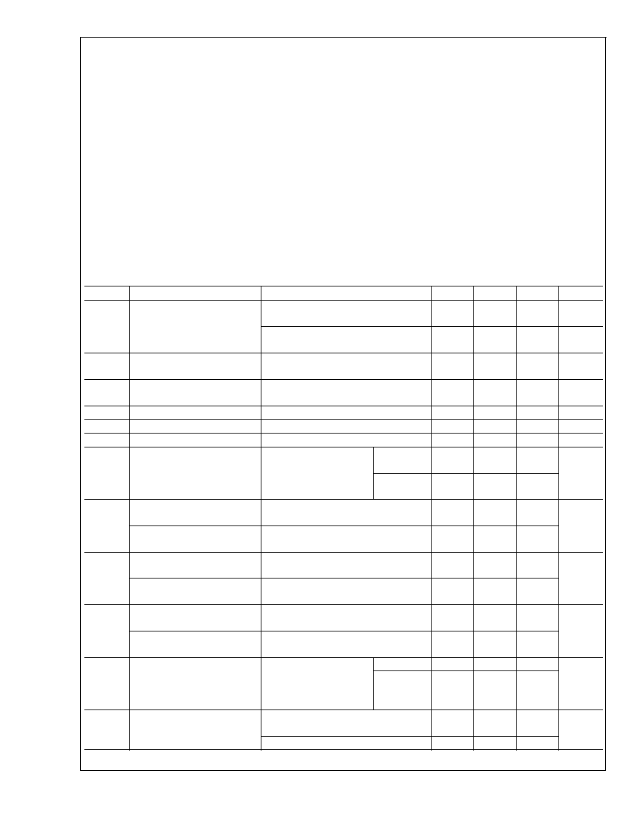
Absolute Maximum Ratings
(Note 1)
If Military/Aerospace specified devices are required,
please contact the National Semiconductor Sales Office/
Distributors for availability and specifications.
ESD Tolerance (Note 2)
Human Body Model
2.5 kV
Machine Model
250V
Supply Voltage
36V (
±
18V)
Input to Output Voltage (Note 3)
±
5V
Input Voltage
±
V
SUPPLY
Output Short-Circuit to GND (Note 4)
Continuous
Storage Temperature Range
-65∞C to +150∞C
Junction Temperature (T
JMAX
)
+150∞C
Lead Temperature
(Soldering, 10 seconds)
260∞C
Power Dissipation
(Note 8)
C
L
Pin to GND Voltage
±
1.2V
Operating Ratings
Operating Temperature Range
-40∞C to +125∞C
Operating Supply Range
5V to
±
16V
Thermal Resistance (
JA
),
PSOP Package (Note 6)
180∞C/W
Thermal Resistance (
JC
)
TO-263 Package
4∞C/W
Thermal Resistance (
JA
)
TO-263 Package
80∞C/W
±
15V Electrical Characteristics
The following specifications apply for Supply Voltage =
±
15V, V
CM
= 0, R
L
100 k and R
S
= 50
, C
L
open, unless otherwise
noted. Boldface limits apply for T
A
= T
J
= T
MIN
to T
MAX
; all other limits T
A
= T
J
= 25∞C.
Symbol
Parameter
Conditions
Min
Typ
Max
Units
A
V
Voltage Gain
R
L
= 1 k
, V
IN
=
±
10V
0.99
0.98
0.995
V/V
R
L
= 50
, V
IN
=
±
10V
0.86
0.84
0.92
V/V
V
OS
Input Offset Voltage
R
L
= 1 k
, R
S
= 0V
±
4
±
35
±
52
mV
I
B
Input Bias Current
V
IN
= 0V, R
L
= 1 k
, R
S
= 0V
±
2
±
15
±
17
µA
R.
IN
Input Resistance
R.
L
= 50
250
k
C
IN
Input Capacitance
3.5
pF
R
O
Output Resistance
I
O
=
±
10 mA
5
I
S
Power Supply Current
R
L
=
, V
IN
= 0
11
14.5
16.5
mA
750 µA into
C
L
Pin
14.9
18.5
20.5
V
O
1
Positive Output Swing
I
O
= 300 mA, R
S
= 0V, V
IN
=
±
V
S
11.2
10.8
11.9
V
Negative Output Swing
I
O
= 300 mA, R
S
= 0V, V
IN
=
±
V
S
-11.3
-10.3
-9.8
V
O
2
Positive Output Swing
R
L
= 1 k
, R
S
= 0V, V
IN
=
±
V
S
13.1
12.9
13.4
V
Negative Output Swing
R
L
= 1 k
, R
S
= 0V, V
IN
=
±
V
S
-13.4
-12.9
-12.6
V
O
3
Positive Output Swing
R
L
= 50
, R
S
= 0V, V
IN
=
±
V
S
11.6
11.2
12.2
V
Negative Output Swing
R
L
= 50
, R
S
= 0V, V
IN
=
±
V
S
-11.9
-10.9
-10.6
V
EF
Error Flag Output Voltage
R
L
=
, V
IN
= 0,
EF pulled up with 5 k
to +5V
Normal
5.00
V
During
Thermal
Shutdown
0.25
T
SH
Thermal Shutdown
Temperature
Measure Quantity is Die (Junction)
Temperature
168
∞C
Hysteresis
10
LMH6321
www.national.com
2

±
15V Electrical Characteristics
(Continued)
The following specifications apply for Supply Voltage =
±
15V, V
CM
= 0, R
L
100 k and R
S
= 50
, C
L
open, unless otherwise
noted. Boldface limits apply for T
A
= T
J
= T
MIN
to T
MAX
; all other limits T
A
= T
J
= 25∞C.
Symbol
Parameter
Conditions
Min
Typ
Max
Units
I
SH
Supply Current at Thermal
Shutdown
EF pulled up with 5 k
to +5V
3
mA
PSSR
Power Supply Rejection Ratio
R
L
= 1 k
, V
IN
= 0V,
V
S
=
±
5V to
±
15V
Positive
58
54
66
dB
Negative
58
54
64
SR
Slew Rate
V
IN
=
±
11V, R
L
= 1 k
2900
V/µs
V
IN
=
±
11V, R
L
= 50
1800
BW
-3 dB Bandwidth
V
IN
=
±
20 mV
PP
, R
L
= 50
110
MHz
LSBW
Large Signal Bandwidth
V
IN
= 2 V
PP
, R
L
= 50
48
MHz
HD2
2
nd
Harmonic Distortion
V
O
= 2 V
PP
, f = 100 kHz
R
L
= 50
-59
dBc
R
L
= 100
-70
V
O
= 2 V
PP
, f = 1 MHz
R
L
= 50
-57
R
L
= 100
-68
HD3
3rd Harmonic Distortion
V
O
= 2 V
PP
, f = 100 kHz
R
L
= 50
-59
dBc
R
L
= 100
-70
V
O
= 2 V
PP
, f = 1 MHz
R
L
= 50
-62
R
L
= 100
-73
e
n
Input Voltage Noise
f
1 MHz
2.8
nV/
i
n
Input Current Noise
f
1 MHz
2.4
pA/
I
SC
1
Output Short Circuit Current
Source (Note 7)
V
O
= 0V,
Program Current
into C
L
= 25 µA
Sourcing
V
IN
= +3V
4.5
4.5
10
15.5
15.5
mA
Sinking
V
IN
= -3V
4.5
4.5
10
15.5
15.5
V
O
= 0V
Program Current
into C
L
= 750 µA
Sourcing
V
IN
= +3V
280
273
295
308
325
mA
Sinking
V
IN
= -3V
280
275
295
310
325
I
SC
2
Output Short Circuit Current
Source
R
S
= 0V, V
IN
= +3V
(Notes 5, 7)
320
300
570
750
920
mA
Output Short Circuit Current
Sink
R
S
= 0V, V
IN
= -3V
(Notes 5, 7)
300
305
515
750
910
V/I Section
CLV
OS
Current Limit Input Offset
Voltage
R
L
= 1 k
, GND = 0V
±
0.5
±
4.0
±
8.0
mV
CLI
B
Current Limit Input Bias
Current
R
L
= 1 k
-0.5
-0.8
-0.2
µA
CL
CMRR
Current Limit Common Mode
Rejection Ratio
R
L
= 1 k
, GND = -13 to +14V
60
56
69
dB
LMH6321
www.national.com
3

±
5V Electrical Characteristics
The following specifications apply for Supply Voltage =
±
5V, V
CM
= 0, R
L
100 k and R
S
= 50
, C
L
Open, unless otherwise
noted. Boldface limits apply for T
A
= T
J
= T
MIN
to T
MAX
; all other limits T
A
= T
J
= 25∞C.
Symbol
Parameter
Conditions
Min
Typ
Max
Units
A
V
Voltage Gain
R
L
= 1 k
, V
IN
=
±
3V
0.99
0.98
0.994
V/V
R
L
= 50
, V
IN
=
±
3V
0.86
0.84
0.92
V
OS
Offset Voltage
R
L
= 1 k
, R
S
= 0V
±
2.5
±
35
±
50
mV
I
B
Input Bias Current
V
IN
= 0V, R
L
= 1 k
, R
S
= 0V
±
2
±
15
±
17
µA
R
IN
Input Resistance
R
L
= 50
250
k
C
IN
Input Capacitance
3.5
pF
R
O
Output Resistance
I
OUT
=
±
10 mA
5
I
S
Power Supply Current
R
L
=
, V
IN
= 0V
10
13.5
14.7
750 µA into CL Pin
14
17.5
19.5
V
O
1
Positive Output Swing
I
O
= 300 mA, R
S
= 0V, V
IN
=
±
V
S
1.3
0.9
1.9
V
Negative Output Swing
I
O
= 300 mA, R
S
= 0V, V
IN
=
±
V
S
-1.3
-0.5
-0.1
V
O
2
Positive Output Swing
R
L
= 1 k
, R
S
= 0V, V
IN
=
±
V
S
3.2
2.9
3.5
V
Negative Output Swing
R
L
= 1 k
, R
S
= 0V, V
IN
=
±
V
S
-3.5
-3.1
-2.9
V
V
O
3
Positive Output Swing
R
L
= 50
, R
S
= 0V, V
IN
=
±
V
S
2.8
2.5
3.1
V
Negative Output Swing
R
L
= 50
, R
S
= 0V, V
IN
=
±
V
S
-3.0
-2.6
-2.4
V
PSSR
Power Supply Rejection Ratio
R
L
= 1 k
, V
IN
= 0,
V
S
=
±
5V to
±
15V
Positive
58
54
66
dB
Negative
58
54
64
I
SC
1
Output Short Circuit Current
V
O
= 0V, Program
Current into C
L
= 25 µA
Sourcing
V
IN
= +3V
4.5
4.5
9
14.0
15.5
mA
Sinking
V
IN
= -3V
4.5
4.5
9
14.0
15.5
V
O
= 0V, Program
Current into C
L
= 750
µA
Sourcing
V
IN
= +3V
275
270
290
305
320
Sinking
V
IN
= -3V
275
270
290
310
320
I
SC
2
Output Short Circuit Current
Source
R
S
= 0V, V
IN
= +3V
(Notes 5, 7)
300
470
mA
Output Short Circuit Current
Sink
R
S
= 0V, V
IN
= -3V
(Notes 5, 7)
300
400
SR
Slew Rate
V
IN
=
±
2 V
PP
, R
L
= 1 k
450
V/µs
V
IN
=
±
2 V
PP
, R
L
= 50
210
BW
-3 dB Bandwidth
V
IN
=
±
20 mV
PP
, R
L
= 50
90
MHz
LSBW
Large Signal Bandwidth
V
IN
= 2 V
PP
, R
L
= 50
39
MHz
T
SD
Thermal Shutdown
Temperature
170
∞C
Hysteresis
10
LMH6321
www.national.com
4

±
5V Electrical Characteristics
(Continued)
The following specifications apply for Supply Voltage =
±
5V, V
CM
= 0, R
L
100 k and R
S
= 50
, C
L
Open, unless otherwise
noted. Boldface limits apply for T
A
= T
J
= T
MIN
to T
MAX
; all other limits T
A
= T
J
= 25∞C.
Symbol
Parameter
Conditions
Min
Typ
Max
Units
V/I Section
CLV
OS
Current Limit Input Offset
Voltage
R
L
= 1 k
, GND = 0V
2.7
+5
±
5.0
mV
CLI
B
Current Limit Input Bias
Current
R
L
= 1 k
, C
L
= 0V
-0.5
-0.6
-0.2
µA
CL
CMRR
Current Limit Common Mode
Rejection Ratio
R
L
= 1 k
, GND = -3V to +4V
60
56
65
dB
Note 1: Absolute Maximum Ratings indicate limits beyond which damage to the device may occur. Operating Ratings indicate conditions for which the device is
intended to be functional, but specific performance is not guaranteed. For guaranteed specifications and the test conditions, see the Electrical Characteristics Table.
Note 2: Human Body Model is 1.5 k
in series with 100 pF. Machine Model is 0 in series with 200 pF.
Note 3: If the input-output voltage differential exceeds
±
5V, internal clamping diodes will turn on. The current through these diodes should be limited to 5 mA max.
Thus for an input voltage of
±
15V and the output shorted to ground, a minimum of 2 k
should be placed in series with the input.
Note 4: The maximum continuous current must be limited to 300 mA. See the Application section for more details.
Note 5: For the condition where the C
L
pin is left open the output current should not be continuous, but instead, should be limited to low duty cycle pulse mode such
that the RMS output current is less than or equal to 300 mA.
Note 6: Soldered to PC board with copper foot print equal to DAP size. Natural convection (no air flow). Board material is FR-4.
Note 7: V
IN
= + or -4V at T
J
= -40∞C.
Note 8: The maximum power dissipation is a function of T
J(MAX)
,
JA
, and T
A
. The maximum allowable power dissipation at any ambient temperature is
P
D
= T
J(MAX)
≠T
A
)/
JA
. See Thermal Management section of the Application Hints.
Ordering Information
Package
Part Number
Package Marking
Transport Media
NSC Drawing
8-Pin PSOP
LMH6321MR
LMH6321MR
95 Units/Rail
MRA08A
LMH6321MRX
2.5k Units Tape and Reel
7-Pin TO-263
LMH6321TS
LMH6321TS
45 Units/Rail
TS7B
LMH6321TSX
500 Units Tape and Reel
LMH6321
www.national.com
5