 | –≠–ª–µ–∫—Ç—Ä–æ–Ω–Ω—ã–π –∫–æ–º–ø–æ–Ω–µ–Ω—Ç: LMH6502MT | –°–∫–∞—á–∞—Ç—å:  PDF PDF  ZIP ZIP |

LMH6502
Wideband, Low Power, Linear-in-dB Variable Gain
Amplifier
General Description
The LMH
TM
6502 is a wideband DC coupled differential input
voltage controlled gain stage followed by a high-speed cur-
rent feedback Op Amp which can directly drive a low imped-
ance load. Gain adjustment range is more than 70dB for up
to 10MHz.
Maximum gain is set by external components and the gain
can be reduced all the way to cut-off. Power consumption is
300mW with a speed of 130MHz. Output referred DC offset
voltage is less than 350mV over the entire gain control
voltage range. Device-to-device Gain matching is within
±
0.6dB at maximum gain. Furthermore, gain at any V
G
is
tested and the tolerance is guaranteed. The output current
feedback Op Amp allows high frequency large signals (Slew
Rate = 1800V/µs) and can also drive heavy load current
(75mA). Differential inputs allow common mode rejection in
low level amplification or in applications where signals are
carried over relatively long wires. For single ended opera-
tion, the unused input can easily be tied to ground (or to a
virtual half-supply in single supply application). Inverting or
non-inverting gains could be obtained by choosing one input
polarity or the other.
To provide ease of use when working with a single supply,
V
G
range is set to be from 0V to +2V relative to pin 11
potential (ground pin). In single supply operation, this ground
pin is tied to a "virtual" half supply.
LMH6502 gain control is linear in dB for a large portion of the
total gain control range. This makes the device suitable for
AGC circuits among other applications. For linear gain con-
trol
applications,
see
the
LMH6503
datasheet.
The
LMH6502 is available in the SOIC-14 and TSSOP-14 pack-
age.
Features
V
S
=
±
5V, T
A
= 25∞C, R
F
= 1k
, R
G
= 174
, R
L
= 100
, A
V
= A
V(MAX)
= 10 Typical values unless specified.
n
-3dB BW
130MHz
n
Gain control BW
100MHz
n
Adjustment range (typical over temp)
70dB
n
Gain matching (limit)
±
0.6dB
n
Slew rate
1800V/µs
n
Supply current (no load)
27mA
n
Linear output current
±
75mA
n
Output voltage (R
L
= 100
)
±
3.2V
n
Input voltage noise
7.7nV/
n
Input current noise
2.4pA/
n
THD (20MHz, R
L
= 100
, V
O
= 2V
PP
)
-53dBc
n
Replacement for CLC520
Applications
n
Variable attenuator
n
AGC
n
Voltage controller filter
n
Video imaging processing
Gain vs. V
G
for Various Temperature
20067706
Typical Application
20067737
A
VMAX
= 10V/V
LMH
TM
is a trademark of National Semiconductor Corporation.
June 2004
LMH6502
W
ideband,
Low
Power
,
Linear-in-dB
V
ariable
Gain
Amplifier
© 2004 National Semiconductor Corporation
DS200677
www.national.com

Absolute Maximum Ratings
(Note 1)
If Military/Aerospace specified devices are required,
please contact the National Semiconductor Sales Office/
Distributors for availability and specifications.
ESD Tolerance (Note 4):
Human Body
2KV
Machine Model
200V
Input Current
±
10mA
V
IN
Differential
±
(V
+
-V
-
)
Output Current
120mA (Note 3)
Supply Voltages (V
+
- V
-
)
12.6V
Voltage at Input/ Output pins
V
+
+0.8V,V
-
- 0.8V
Storage Temperature Range
-65∞C to +150∞C
Junction Temperature
+150∞C
Soldering Information:
Infrared or Convection (20 sec)
235∞C
Wave Soldering (10 sec)
260∞C
Operating Ratings
(Note 1)
Supply Voltages (V
+
- V
-
)
5V to 12V
Temperature Range
-40∞C to +85∞C
Thermal Resistance:
(
JC
)
(
JA
)
14-Pin SOIC
45∞C/W
138∞C/W
14-Pin TSSOP
51∞C/W
160∞C/W
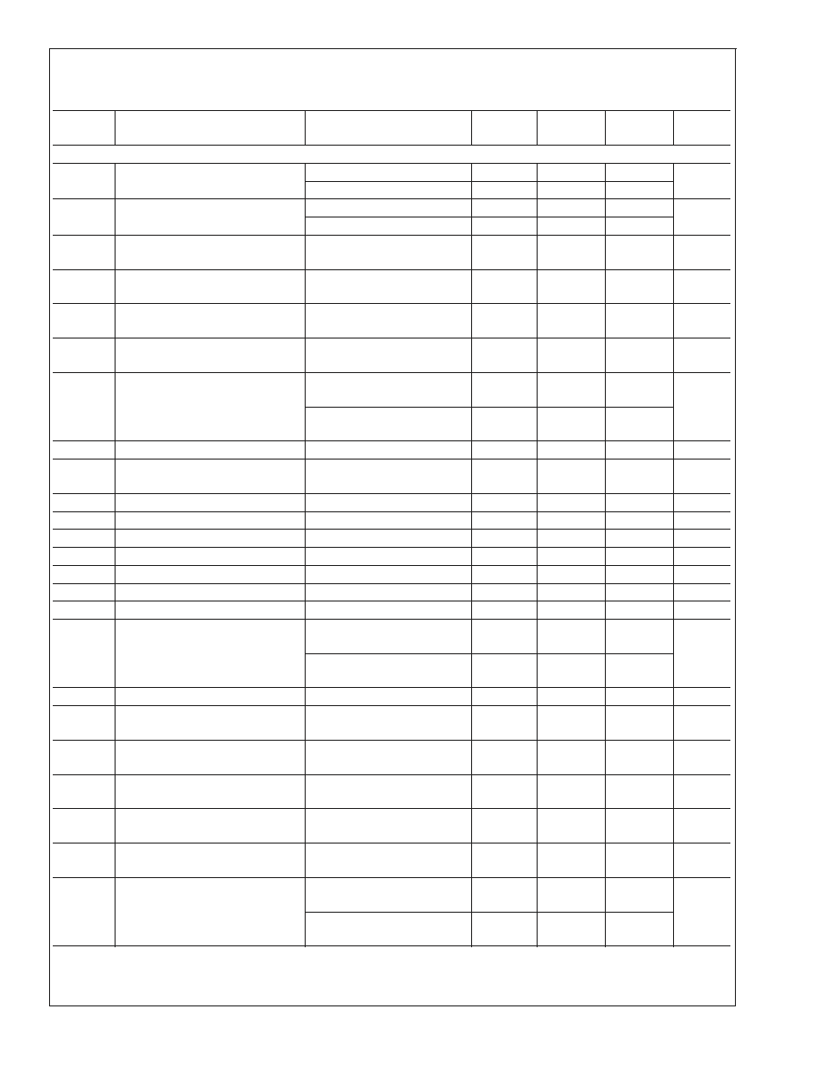
Electrical Characteristics
(Note 2)
Unless otherwise specified, all limits guaranteed for T
J
= 25∞C, V
S
=
±
5V, A
V(MAX)
= 10, V
CM
= 0V, R
F
= 1k
, R
G
= 174
,
V
IN_DIFF
=
±
0.1V, R
L
= 100
, V
G
= +2V. Boldface limits apply at the temperature extremes.
Symbol
Parameter
Conditions
Min
(Note 6)
Typ
(Note 6)
Max
(Note 6)
Units
Frequency Domain Response
BW
-3dB Bandwidth
V
OUT
<
0.5
PP
130
MHz
V
OUT
<
0.5
PP
, A
V(MAX)
= 100
50
GF
Gain Flatness
V
OUT
<
0.5V
PP
0.6V
V
G
2V,
±
0.3dB
30
MHz
Att Range Flat Band (Relative to Max Gain)
Attenuation Range (Note 14)
±
0.2dB, f
<
30MHz
16
dB
±
0.1dB, f
<
30MHz
7.5
BW
Control
Gain control Bandwidth
V
G
= 1V (Note 13)
100
MHz
PL
Linear Phase Deviation
DC to 60MHz
1.5
deg
G Delay
Group Delay
DC to 130MHz
2.5
ns
CT (dB)
Feed-through
V
G
= 0V, 30MHz (Output
Referred)
-47
dB
GR
Gain Adjustment Range
f
<
10MHz
72
dB
f
<
30MHz
67
Time Domain Response
t
r
, t
f
Rise and Fall Time
0.5V Step
2.2
ns
OS %
Overshoot
0.5V Step
10
%
SR
Slew Rate
4V Step
1800
V/µs
G Rate Gain Change Rate
V
IN
= 0.3V, 10%-90% of Final
Output
4.8
dB/ns
Distortion & Noise Performance
HD2
2
nd
Harmonic Distortion
2V
PP
, 20MHz
-55
dBc
HD3
3
rd
Harmonic Distortion
2V
PP
, 20MHz
-57
dBc
THD
Total Harmonic Distortion
2V
PP
, 20MHz
-53
dBc
En tot
Total Equivalent Input Noise
1MHz to 150MHz
7.7
nV/
I
N
Input Noise Current
1MHz to 150MHz
2.4
pA/
DG
Differential Gain
f = 4.43MHz, R
L
= 150
,
Neg. Sync
0.34
%
DP
Differential Phase
f = 4.43MHz, R
L
= 150
,
Neg. Sync
0.10
deg
LMH6502
www.national.com
2
Electrical Characteristics
(Note 2) (Continued)
Unless otherwise specified, all limits guaranteed for T
J
= 25∞C, V
S
=
±
5V, A
V(MAX)
= 10, V
CM
= 0V, R
F
= 1k
, R
G
= 174
,
V
IN_DIFF
=
±
0.1V, R
L
= 100
, V
G
= +2V. Boldface limits apply at the temperature extremes.
Symbol
Parameter
Conditions
Min
(Note 6)
Typ
(Note 6)
Max
(Note 6)
Units
DC & Miscellaneous Performance
GACCU
Gain Accuracy (See Application
Note)
V
G
= 2.0V
0.0
+0.6
dB
1V
<
V
G
<
2V
+0.6/-0.3
+3.1/-3.6
G Match
Gain Matching (See Application
Note)
V
G
= 2.0V
≠
±
0.6
dB
1
<
V
G
<
2V
≠
+2.8/-3.9
K
Gain Multiplier
(See Application Notes)
1.61
1.58
1.72
1.84
1.91
V/V
V
CM
Input Voltage Range
Pin 3 & 6 Common Mode,
|CMRR|
>
55dB (Note 9)
±
2.0
±
1.70
±
2.2
V
V
IN_DIFF
Differential Input Voltage
Between pins 3 & 6
±
0.3
±
0.12
±
0.39
V
I
RG_MAX
R
G
Current
Pins 4 & 5
±
1.70
±
1.56
±
2.22
mA
I
BIAS
Bias Current
Pins 3 & 6(Note 7)
9
18
20
µA
Pins 3 & 6 (Note 7),
V
S
=
±
2.5V
2.5
5
6
TC I
BIAS
Bias Current Drift
Pin 3 & 6(Note 8)
100
nA/∞C
I
OFF
Offset Current
Pin 3 & 6
0.01
2.0
3.6
µA
TC I
OFF
Offset Current Drift
(Note 8)
5
nA/∞C
R
IN
Input Resistance
Pin 3 & 6
750
k
C
IN
Input Capacitance
Pin 3 & 6
5
pF
I
VG
V
G
Bias Current
Pin 2, V
G
= 0V(Note 7)
-300
µA
TC I
VG
V
G
Bias Drift
Pin 2(Note 8)
20
nA/∞C
R
VG
V
G
Input Resistance
Pin 2
10
k
C
VG
V
G
Input Capacitance
Pin 2
1.3
pF
V
OUT
Output Voltage Range
R
L
= 100
±
3.00
±
2.95
±
3.20
V
R
L
= Open
±
3.95
±
3.82
±
4.00
R
OUT
Output Impedance
DC
0.1
I
OUT
Output Current
V
OUT
=
±
4V from Rails
±
80
±
75
±
90
mA
V
O
OFFSET
Output Offset Voltage
0V
<
V
G
<
2V
±
80
±
300
±
380
mV
+PSRR
+Power Supply Rejection Ratio
(Note 10)
Input Referred, 1V change,
V
G
= 2.2V
-69
-47
-45
dB
-PSRR
-Power Supply Rejection Ratio
(Note 10)
Input Referred, 1V change,
V
G
= 2.2V
-58
-41
-40
dB
CMRR
Common Mode Rejection Ratio
(Note 9)
Input Referred,V
G
= 2V
-1.8V
<
V
CM
<
1.8V
-72
dB
I
S
Supply Current
No Load
27
38
41
mA
V
S
=
±
2.5V, R
L
= Open
9.3
16
19
LMH6502
www.national.com
3

Electrical Characteristics
(Note 2) (Continued)
Note 1: Absolute Maximum Ratings indicate limits beyond which damage to the device may occur. Operating Ratings indicate conditions for which the device is
intended to be functional, but specific performance is not guaranteed. For guaranteed specifications, see the Electrical Characteristics tables.
Note 2: Electrical Table values apply only for factory testing conditions at the temperature indicated. Factory testing conditions result in very limited self-heating of
the device such that T
J
= T
A
. No guarantee of parametric performance is indicated in the electrical tables under conditions of internal self-heating where T
J
>
T
A
.
Note 3: The maximum output current (I
OUT
) is determined by device power dissipation limitations or value specified, whichever is lower.
Note 4: Human body model: 1.5k
in series with 100pF. Machine model: 0 in series with 200pF.
Note 5: Slew Rate is the average of the rising and falling rates.
Note 6: Typical values represent the most likely parametric norm. Bold numbers refer to over temperature limits.
Note 7: Positive current corresponds to current flowing in the device.
Note 8: Drift determined by dividing the change in parameter distribution average at temperature extremes by the total temperature change.
Note 9: CMRR definition: [|
V
OUT
/
V
CM
| / A
V
] with 0.1V differential input voltage.
Note 10: +PSRR definition: [|
V
OUT
/
V
+
| / A
V
], -PSRR definition: [|
V
OUT
/
V
-
| / A
V
] with 0.1V differential input voltage.
Note 11: Gain/Phase normalized to low frequency value at 25∞C.
Note 12: Gain/Phase normalized to low frequency value at each A
V
.
Note 13: Gain Control Frequency Response Schematic:
20067738
Note 14: Flat Band Attenuation (Relative to Max Gain) Range Definition: Specified as the attenuation range from maximum which allows gain flatness specified
(either
±
0.2dB or
±
0.1dB) relative to A
VMAX
gain. For example, for f
<
30MHz, here are the Flat Band Attenuation ranges:
±
0.2dB
20dB down to 4dB = 16dB range
±
0.1dB
20dB down to 12.5 dB = 7.5dB range
Connection Diagram
14-Pin SOIC/TSSOP
20067736
Top View
Ordering Information
Package
Part Number
Package Marking
Transport Media
NSC Drawing
14-pin SOIC
LMH6502MA
LMH6502MA
55 Units/Rail
M14A
LMH6502MAX
2.5k Units Tape and Reel
14-Pin TSSOP
LMH6502MT
LMH6502MT
94 Units/Rail
MTC14
LMH6502MTX
2.5k Units Tape and Reel
LMH6502
www.national.com
4
Typical Performance Characteristics
Unless otherwise specified: V
S
=
±
5V, 25∞C, V
G
= V
GMAX
,
V
CM
= 0V, R
F
= 1k
, R
G
= 174
, both inputs terminated in 50, R
L
= 100
, Typical values, results referred to device output.
Small Signal Frequency for Various V
G
Large Signal Frequency for Various V
G
20067731
20067732
Frequency Response Over Temperature (A
V
= 10)
Frequency Response for Various V
G
(A
VMAX
= 10)
20067707
20067708
Frequency Response for Various V
G
(A
VMAX
= 10)
(
±
2.5V)
Small Signal Frequency Response for Various A
VMAX
20067714
20067723
LMH6502
www.national.com
5

Typical Performance Characteristics
Unless otherwise specified: V
S
=
±
5V, 25∞C, V
G
= V
GMAX
, V
CM
= 0V, R
F
= 1k
, R
G
= 174
, both inputs terminated in 50, R
L
= 100
, Typical values, results referred to device
output. (Continued)
Large Signal Frequency Response for Various A
VMAX
Frequency Response for Various V
G
(A
VMAX
= 100)
(Small Signal)
20067724
20067729
Frequency Response for Various V
G
(A
VMAX
= 100)
(Large Signal)
I
S
vs. V
S
20067730
20067750
I
S
vs. V
S
Input Bias Current vs. V
S
20067751
20067752
LMH6502
www.national.com
6

Typical Performance Characteristics
Unless otherwise specified: V
S
=
±
5V, 25∞C, V
G
= V
GMAX
, V
CM
= 0V, R
F
= 1k
, R
G
= 174
, both inputs terminated in 50, R
L
= 100
, Typical values, results referred to device
output. (Continued)
A
VMAX
vs. V
CM
A
VMAX
vs. V
CM
20067767
20067766
PSRR
±
5V
PSRR
±
2.5V
20067703
20067704
CMRR
±
5V
CMRR
±
2.5V
20067701
20067702
LMH6502
www.national.com
7

Typical Performance Characteristics
Unless otherwise specified: V
S
=
±
5V, 25∞C, V
G
= V
GMAX
, V
CM
= 0V, R
F
= 1k
, R
G
= 174
, both inputs terminated in 50, R
L
= 100
, Typical values, results referred to device
output. (Continued)
A
VMAX
vs. Supply Voltage
Supply Current vs. V
CM
20067768
20067756
Supply Current vs. V
CM
Output Offset Voltage vs. V
CM
(Typical Unit #1)
20067757
20067758
Output Offset Voltage vs. V
CM
(Typical Unit #2)
Output Offset Voltage vs. V
CM
(Typical Unit #3)
20067759
20067760
LMH6502
www.national.com
8

Typical Performance Characteristics
Unless otherwise specified: V
S
=
±
5V, 25∞C, V
G
= V
GMAX
, V
CM
= 0V, R
F
= 1k
, R
G
= 174
, both inputs terminated in 50, R
L
= 100
, Typical values, results referred to device
output. (Continued)
Feed through Isolation
Gain Flatness and Linear Phase Deviation vs. V
G
20067721
20067709
Gain Flatness Frequency vs. Gain (Note 14)
Group Delay vs. Frequency
20067711
20067712
K Factor vs. R
G
Gain vs. V
G
Including Limits
20067739
20067705
LMH6502
www.national.com
9

Typical Performance Characteristics
Unless otherwise specified: V
S
=
±
5V, 25∞C, V
G
= V
GMAX
, V
CM
= 0V, R
F
= 1k
, R
G
= 174
, both inputs terminated in 50, R
L
= 100
, Typical values, results referred to device
output. (Continued)
BW vs. R
F
Gain vs. V
G
(
±
5V)
20067740
20067706
Gain vs. V
G
(
±
2.5V)
Output Offset Voltage vs. V
G
(Typical Unit #1)
20067713
20067753
Output Offset Voltage vs. V
G
(Typical Unit #2)
Output Offset Voltage vs. V
G
(Typical Unit #3)
20067754
20067755
LMH6502
www.national.com
10
Typical Performance Characteristics
Unless otherwise specified: V
S
=
±
5V, 25∞C, V
G
= V
GMAX
, V
CM
= 0V, R
F
= 1k
, R
G
= 174
, both inputs terminated in 50, R
L
= 100
, Typical values, results referred to device
output. (Continued)
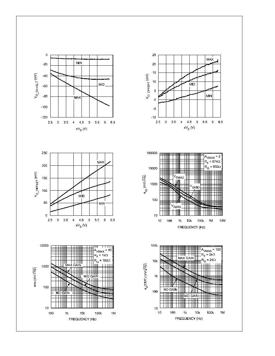
Output Offset Voltage vs.
±
V
S
for various V
G
(Typical Unit# 1)
Output Offset Voltage vs.
±
V
S
for various V
G
(Typical Unit# 2)
20067761
20067762
Output Offset Voltage vs.
±
V
S
for various V
G
(Typical Unit# 3)
Noise vs. Frequency (A
VMAX
= 2)
20067763
20067725
Noise vs. Frequency (A
VMAX
= 10)
Noise vs. Frequency (A
VMAX
= 100)
20067710
20067717
LMH6502
www.national.com
11

Typical Performance Characteristics
Unless otherwise specified: V
S
=
±
5V, 25∞C, V
G
= V
GMAX
, V
CM
= 0V, R
F
= 1k
, R
G
= 174
, both inputs terminated in 50, R
L
= 100
, Typical values, results referred to device
output. (Continued)
-1dB Compression
Output Voltage vs. Output Current
20067722
20067726
HD2 & HD3 vs. P
OUT
THD vs. P
OUT
20067733
20067718
THD vs. P
OUT
HD2 & HD3 vs. V
G
20067719
20067728
LMH6502
www.national.com
12

Typical Performance Characteristics
Unless otherwise specified: V
S
=
±
5V, 25∞C, V
G
= V
GMAX
, V
CM
= 0V, R
F
= 1k
, R
G
= 174
, both inputs terminated in 50, R
L
= 100
, Typical values, results referred to device
output. (Continued)
THD vs. V
G
THD vs. V
G
20067720
20067715
V
G
Bias Current vs. V
G
Step Response Plot
20067727
20067734
Step Response Plot
Gain vs. V
G
Step
20067735
20067764
LMH6502
www.national.com
13

Typical Performance Characteristics
Unless otherwise specified: V
S
=
±
5V, 25∞C, V
G
= V
GMAX
, V
CM
= 0V, R
F
= 1k
, R
G
= 174
, both inputs terminated in 50, R
L
= 100
, Typical values, results referred to device
output. (Continued)
Feedthrough from V
G
20067765
Application Information
THEORY OF OPERATION
A simplified schematic is shown in Figure 1. +V
IN
and -V
IN
are buffered with closed loop voltage followers inducing a
signal current in Rg proportional to (+V
IN
) - (-V
IN
), the dif-
ferential input voltage. This current controls a current source
which supplies two well-matched transistor, Q1 and Q2.
The current flowing through Q2 is converted to the final
output voltage using R
F
and the output amplifier, U1. By
changing the fraction of the signal current "I" which flows
through Q2, the gain is changed. This is done by changing
the voltage applied differentially to the bases of Q1 and Q2.
For example, with V
G
= 0V, Q1 conducts heavily and Q2 is
off. With none of "I" flowing through R
F
, the LMH6502's input
to output gain is strongly attenuated. With V
G
= +2V, Q1 is off
and the entire signal current flows through Q2 to R
F
produc-
ing maximum gain. With V
G
set to 1V, the bases of Q1 and
Q2 are set to approximately the same voltage, Q1 and Q2
have the same collector currents - equal to one half of the
signal current "I", thus the gain is approximately one half the
maximum gain.
CHOOSING R
F
& R
G
Maximum input amplitude and maximum gain are the two
key specifications that determine component values in a
LMH6502 application.
The output stage op amp is a current-feedback type amplifier
optimized for R
F
= 1k
. R
G
can then be computed as:
(1)
To determine whether the maximum input amplitude will
overdrive the LMH6502, compute:
V
DMAX
= (R
G
+ 3.0
) x 1.70mA
(2)
the maximum differential input voltage for linear operation. If
the maximum input amplitude exceeds the above V
DMAX
limit, then LMH6502 should either be moved to a location in
the signal chain where input amplitudes are reduced, or the
LMH6502 gain A
VMAX
should be reduced or the values for
R
G
and R
F
should be increased. The overall system perfor-
mance impact is different based on the choice made. If the
input amplitude is reduced, re-compute the impact on signal-
to-noise ratio. If A
VMAX
is reduced, post LMH6502 amplifier
gain, should be increased, or another gain stage added to
make up for reduced system gain. To increase R
G
and R
F
,
compute the lowest acceptable value for R
G
:
R
G
>
590 x V
DMAX
- 3
(3)
Operating with R
G
larger than this value insures linear op-
eration of the input buffers.
R
F
may be computed from selected R
G
and A
VMAX
: R
F
should be
>
= 1k
for overall best performance, however R
F
<
1k
can be implemented if necessary using a loop gain
reducing resistor to ground on the inverting summing node of
the output amplifier (see application note QA-13 for details).
ADJUSTING OFFSET
Offset can be broken into two parts; an input-referred term
and an output-referred term. The input-referred offset shows
up as a variation in output voltage as V
G
is changed. This
can be trimmed using the circuit in Figure 2 by placing a low
frequency square wave (V
LOW
= 0V, V
HIGH
= 2V into V
G
with
20067741
FIGURE 1. LMH6502 Block Diagram
LMH6502
www.national.com
14

Application Information
(Continued)
V
IN
= 0V, the input referred V
OS
term shows up as a small
square wave riding a DC value. Adjust R
10
to null the V
OS
square wave term to zero. After adjusting the input-referred
offset, adjust R
14
(with V
IN
= 0, V
G
= 0) until V
OUT
is zero.
Finally, for inverting applications V
IN
may be applied to pin 6
and the offset adjustment to pin 3. These steps will minimize
the output offset voltage. However, since the offset term itself
varies with the gain setting, the correction is not perfect and
some residual output offset will remain at in-between V
G
's.
Also, this offset trim does not improve output offset tempera-
ture coefficient.
GAIN ACCURACY
Defined as the actual gain compared against the theoretical
gain at a certain V
G
(results expressed in dB).
Theoretical gain is given by:
(4)
Where K = 1.72 (nominal) & V
C
= 90mV
@
room tempera-
ture.
For a V
G
range, the value specified in the tables represents
the worst case accuracy over the entire range. The "Typical"
value would be the worst case difference between the "Typi-
cal Gain" and the "Theoretical gain". The "Max" value would
be the worst case difference between the max/min gain limit
and the "Theoretical gain".
GAIN MATCHING
Defined as the limit on gain variation at a certain V
G
(ex-
pressed in dB). Specified as "Max" only (no "Typical"). For a
V
G
range, the value specified represents the worst case
matching over the entire range. The "Max" value would be
the worst case difference between the max/min gain limit
and the typical gain.
NOISE
Figure 3 describes the LMH6502's output-referred spot
noise density as a function of frequency with A
VMAX
= 10V/V.
The plot includes all the noise contributing terms. However,
with both inputs terminated in 50
, the input noise contribu-
tion is minimal. At A
VMAX
= 10V/V, the LMH6502 has a typical
input-referred spot noise density (e
in
) of 7.7nV/
flat-
band. For applications extending well into the flat-band re-
gion, the input RMS voltage noise can be determined from
the following single-pole model:
(5)
CIRCUIT LAYOUT CONSIDERATIONS & EVALUATION
BOARD
A good high frequency PCB layout including ground plane
construction and power supply bypassing close to the pack-
age are critical to achieving full performance. The amplifier is
sensitive to stray capacitance to ground at the I
-
input (pin
12); keep node trace area small. Shunt capacitance across
the feedback resistor should not be used to compensate for
this effect. For best performance at low maximum gains
(A
VMAX
<
10) +R
G
and -R
G
connections should be treated in
a similar fashion. Capacitance to ground should be mini-
mized by removing the ground plane from under the body of
R
G.
. Parasitic or load capacitance directly on the output (pin
10) degrades phase margin leading to frequency response
peaking.
The LMH6502 is fully stable when driving a 100
load. With
reduced load (e.g. 1k
) there is a possibility of instability at
very high frequencies beyond 400MHz especially with a
capacitive load. When the LMH6502 is connected to a light
load as such, it is recommended to add a snubber network to
the output (e.g. 100
and 39pF in series tied between the
LMH6502 output and ground). C
L
can also be isolated from
the output by placing a small resistor in series with the output
(pin 10).
Component parasitics also influence high frequency results.
Therefore it is recommended to use metal film resistors such
as RN55D or leadless components such as surface mount
devices. High profile sockets are not recommended.
20067743
FIGURE 2. Nulling the output offset voltage
20067710
FIGURE 3. Output Referred Voltage Noise vs.
Frequency
LMH6502
www.national.com
15

Application Information
(Continued)
National Semiconductor suggests the following evaluation
boards as a guide for high frequency layout and as an aid in
device testing and characterization:
Device
Package
Evaluation Board
Part Number
LMH6502MA
SOIC-14
CLC730033
LMH6502MT
TSSOP-14
CLC730146
The evaluation board is shipped when a device sample
request is placed with National Semiconductor
SINGLE SUPPLY OPERATION
It is possible to operate the LMH6502 with a single supply. To
do so, tie pin 11 (GND) to a potential about mid point
between V
+
and V
-
. Two examples are shown in Figure 4 &
Figure 5.
OPERATING AT LOWER SUPPLY VOLTAGES
The LMH6502 is rated for operation down to 5V supplies (V
+
-V
-
). There are some specifications shown for operation at
±
2.5V within the data sheet (i.e. Frequency Response,
CMRR, PSRR, Gain vs. V
G
, etc.). Compared to
±
5V opera-
tion, at lower supplies:
a) V
G
range shifts lower.
Here are the approximate expressions for various V
G
voltages as a function of V
+
:
TABLE 1. V
G
Definition Based on V
+
V
G
Definition
Expression (V)
V
G_MIN
Gain Cut-off
0.2 x V
+
-1
V
G_MID
A
VMAX
/2
0.2 x V
+
V
G_MAX
A
VMAX
0.2 x V
+
+1
b) V
G_LIMIT
(maximum permissible voltage on V
G
) is re-
duced. This is due to limitations within the device arising
from transistor headroom. Beyond this limit, device per-
formance will be affected (non-destructive). This could
reveal itself as premature high frequency response roll-
off. With
±
2.5V supplies, V
G_LIMIT
is below 1.1V whereas
V
G
= 1.5V is needed to get maximum gain. This means
that operating under these conditions has reduced the
maximum permissible voltage on V
G
to a level below
what is needed to get Max gain. If supply voltages are
asymmetrical with V
+
being lower, further "pinching" of
V
G
range could result; for example, with V
+
= 2V, and V
-
= -3V, V
G_LIMIT
= 0.40V which results in maximum gain
being 2.5dB less than what would be expected when V
S
is higher.
c) "Max_gain" reduces. There is an intrinsic reduction in
max gain when the total supply voltage is reduced (see
Typical Performance Characteristics plots for Gain vs. V
G
(V
S
=
±
2.5V). In addition, there is the more drastic
mechanism described in "b" above. Beyond V
G_LIMIT
,
high frequency response is also effected.
Application Circuits
AGC LOOP
Figure 6 shows a typical AGC circuit. The LMH6502 is
followed up with a LMH6714 for higher overall gain. The
output of the LMH6714 is rectified and fed to an inverting
integrator using a LMH6657 (wideband voltage feedback op
amp). When the output voltage, V
OUT
, is too large the inte-
grator output voltage ramps down reducing the net gain of
the LMH6502 and V
OUT
. If the output voltage is too small,
the integrator ramps up increasing the net gain and the
output voltage. Actual output level is set with R
1
. To prevent
shifts in DC output voltage with DC changes in input signal
level, trim pot R
2
is provided. AGC circuits are always limited
in the range of input signals over which constant output level
can be maintained. In this circuit, we would expect that
reasonable AGC action could be maintained for at least
40dB. In practice, rectifier dynamic range limits reduce this
slightly.
20067746
FIGURE 4. AC Coupled Single Supply VGA
20067747
FIGURE 5. Transformer Coupled Single Supply VGA
LMH6502
www.national.com
16

Application Circuits
(Continued)
FREQUENCY SHAPING
Frequency Shaping Frequency shaping and bandwidth extension of the LMH6502 can be accomplished using parallel networks
connected across the R
G
ports. The network shown in the Figure 7 schematic will effectively extend the LMH6502's bandwidth.
20067748
FIGURE 6. Automatic Gain Control (AGC) Loop
20067749
FIGURE 7. Frequency Shaping
LMH6502
www.national.com
17

Physical Dimensions
inches (millimeters) unless otherwise noted
14-Pin SOIC
NS Package Number M14A
14-Pin TSSOP
NS Package Number MTC14
LMH6502
www.national.com
18

Notes
LIFE SUPPORT POLICY
NATIONAL'S PRODUCTS ARE NOT AUTHORIZED FOR USE AS CRITICAL COMPONENTS IN LIFE SUPPORT
DEVICES OR SYSTEMS WITHOUT THE EXPRESS WRITTEN APPROVAL OF THE PRESIDENT AND GENERAL
COUNSEL OF NATIONAL SEMICONDUCTOR CORPORATION. As used herein:
1. Life support devices or systems are devices or
systems which, (a) are intended for surgical implant
into the body, or (b) support or sustain life, and
whose failure to perform when properly used in
accordance with instructions for use provided in the
labeling, can be reasonably expected to result in a
significant injury to the user.
2. A critical component is any component of a life
support device or system whose failure to perform
can be reasonably expected to cause the failure of
the life support device or system, or to affect its
safety or effectiveness.
BANNED SUBSTANCE COMPLIANCE
National Semiconductor certifies that the products and packing materials meet the provisions of the Customer Products
Stewardship Specification (CSP-9-111C2) and the Banned Substances and Materials of Interest Specification
(CSP-9-111S2) and contain no ``Banned Substances'' as defined in CSP-9-111S2.
National Semiconductor
Americas Customer
Support Center
Email: new.feedback@nsc.com
Tel: 1-800-272-9959
National Semiconductor
Europe Customer Support Center
Fax: +49 (0) 180-530 85 86
Email: europe.support@nsc.com
Deutsch Tel: +49 (0) 69 9508 6208
English
Tel: +44 (0) 870 24 0 2171
FranÁais Tel: +33 (0) 1 41 91 8790
National Semiconductor
Asia Pacific Customer
Support Center
Email: ap.support@nsc.com
National Semiconductor
Japan Customer Support Center
Fax: 81-3-5639-7507
Email: jpn.feedback@nsc.com
Tel: 81-3-5639-7560
www.national.com
LMH6502
W
ideband,
Low
Power
,
Linear-in-dB
V
ariable
Gain
Amplifier
National does not assume any responsibility for use of any circuitry described, no circuit patent licenses are implied and National reserves the right at any time without notice to change said circuitry and specifications.