Äîêóìåíòàöèÿ è îïèñàíèÿ www.docs.chipfind.ru
LMH6503
Wideband, Low Power, Linear Variable Gain Amplifier
General Description
The LMH
TM
6503 is a wideband DC coupled differential input
voltage controlled gain stage followed by a high-speed cur-
rent feedback Op Amp which can directly drive a low imped-
ance load. Gain adjustment range is more than 70dB for up
to 10MHz.
Maximum gain is set by external components and the gain
can be reduced all the way to cut-off. Power consumption is
370mW with a speed of 135MHz . Output referred DC offset
voltage is less than 350mV over the entire gain control
voltage range. Device-to-device Gain matching is within
0.7dB at maximum gain. Furthermore, gain at any V
G
is
tested and the tolerance is guaranteed. The output current
feedback Op Amp allows high frequency large signals (Slew
Rate = 1800V/µs) and can also drive heavy load current
(75mA). Differential inputs allow common mode rejection in
low level amplification or in applications where signals are
carried over relatively long wires. For single ended opera-
tion, the unused input can easily be tied to ground (or to a
virtual half-supply in single supply application). Inverting or
non-inverting gains could be obtained by choosing one input
polarity or the other.
To further increase versatility when used in a single supply
application, gain control range is set to be from -1V to +1V
relative to pin 11 potential (ground pin). In single supply
operation, this ground pin is tied to a "virtual" half supply.
Gain control pin has high input impedance to simplify its
drive requirement. Gain control is linear in V/V throughout
the gain adjustment range. Maximum gain can be set to be
anywhere between 1V/V to 100V/V or higher. For linear in dB
gain control applications, see LMH6502 datasheet.
The LMH6503 is available in the SOIC-14 and TSSOP-14
package.
Features
V
S
=
±
5V, T
A
= 25°C, R
F
= 1k
, R
G
= 174
, R
L
= 100
, A
V
= A
V(MAX)
= 10, Typical values unless specified.
n
-3dB BW
135MHz
n
Gain control BW
100MHz
n
Adjustment range (typical over temp)
70dB
n
Gain matching (limit)
±
0.7dB
n
Slew rate
1800V/µs
n
Supply current (no load)
37mA
n
Linear output current
±
75mA
n
Output voltage (R
L
= 100
)
±
3.2V
n
Input voltage noise
6.6nV/
n
Input current noise
2.4pA/
n
THD (20MHz, R
L
= 100
, V
O
= 2V
PP
)
-57dBc
n
Replacement for CLC522
Applications
n
Variable attenuator
n
AGC
n
Voltage controller filter
n
Multiplier
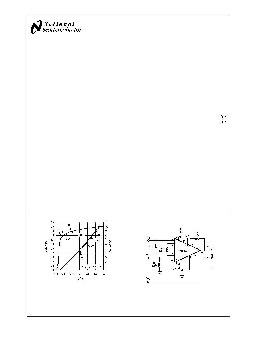
20073913
Gain vs. V
G
for Various Temperature
Typical Application
20073933
A
VMAX
= 10V/V
LMH
TM
is a trademark of National Semiconductor Corporation.
June 2004
LMH6503
W
ideband,
Low
Power
,
Linear
V
ariable
Gain
Amplifier
© 2004 National Semiconductor Corporation
DS200739
www.national.com
Absolute Maximum Ratings
(Note 1)
If Military/Aerospace specified devices are required,
please contact the National Semiconductor Sales Office/
Distributors for availability and specifications.
ESD Tolerance: (Note 4)
Human Body
2KV
Machine Model
200V
Input Current
±
10mA
V
IN
Differential
±
(V
+
-V
-
)
Output Current
120mA (Note 3)
Supply Voltages (V
+
- V
-
)
12.6V
Voltage at Input/ Output pins
V
+
+0.8V,V
-
- 0.8V
Soldering Information:
Infrared or Convection (20 sec)
235°C
Wave Soldering (10 sec)
260°C
Storage Temperature Range
-65°C to +150°C
Junction Temperature
+150°C
Operating Ratings
(Note 1)
Supply Voltages (V
+
- V
-
)
5V to 12V
Temperature Range
-40°C to +85°C
Thermal Resistance:
JA
JC
14-Pin SOIC
138°C/W
45°C/W
14-Pin TSSOP
160°C/W
51°C/W
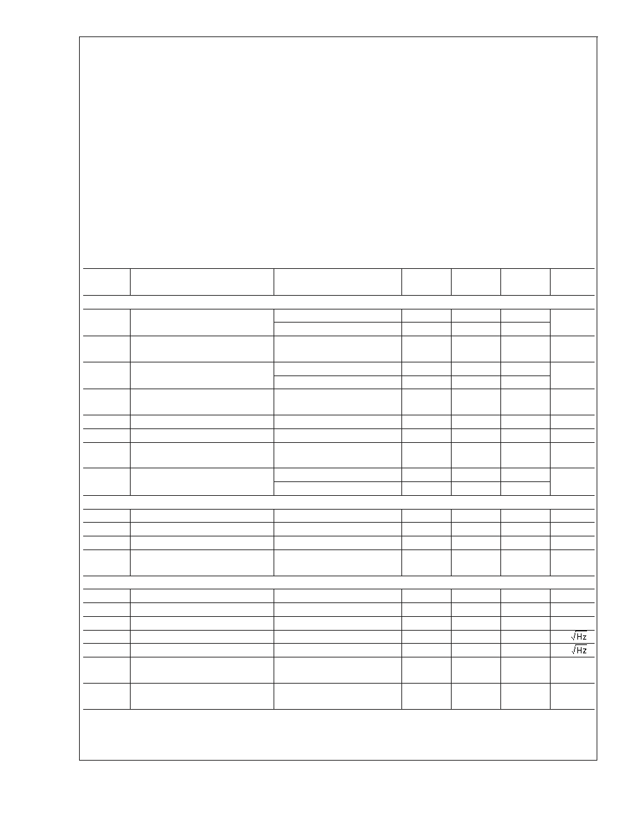
Electrical Characteristics
(Note 2)
Unless otherwise specified, all limits guaranteed for T
J
= 25°C, V
S
=
±
5V, A
V(MAX)
= 10, V
CM
= 0V, R
F
= 1k
, R
G
= 174
, V
IN-
_DIFF
=
±
0.1V, R
L
= 100
, V
G
= +1V. Boldface limits apply at the temperature extremes.
Symbol
Parameter
Conditions
Min
(Note 6)
Typ
(Note 6)
Max
(Note 6)
Units
Frequency Domain Response
BW
-3dB Bandwidth
V
OUT
<
0.5
PP
135
MHz
V
OUT
<
0.5
PP
, A
V(MAX)
= 100
50
GF
Gain Flatness
V
OUT
<
0.5V
PP
,
-1V
<
V
G
<
1V,
±
0.2dB
40
MHz
Att Range Flat Band (Relative to Max Gain)
Attenuation Range (Note 13)
±
0.2dB Flatness, f
<
30MHZ
20
MHz
±
0.1dB, f
<
30MHZ
6.6
BW
Control
Gain Control Bandwidth
V
G
= 0V (Note 11)
100
MHz
PL
Linear Phase Deviation
DC to 60MHz
1.6
deg
G Delay
Group Delay
DC to 130MHz
2.6
ns
CT (dB)
Feed-through
V
G
= -1.2V, 30MHz (Output
Referred)
-48
dB
GR
Gain Adjustment Range
f
<
10MHz
79
dB
f
<
30MHz
68
Time Domain Response
t
r
, t
f
Rise and Fall Time
0.5V Step
2.2
ns
OS%
Overshoot
0.5V Step
10
%
SR
Slew Rate
4V Step (Note 5)
1800
V/µs
G Rate
Gain Change Rate
V
IN
= 0.3V, 10%-90% of final
output
4.6
dB/ns
Distortion & Noise performance
HD2
2
nd
Harmonic Distortion
2V
PP
, 20MHz
-60
dBc
HD3
3
rd
Harmonic Distortion
2V
PP
, 20MHz
-61
dBc
THD
Total Harmonic Distortion
2V
PP
, 20MHz
-57
dBc
En tot
Total Equivalent Input Noise
1MHz to 150MHz
6.6
nV/
I
n
Input Noise Current
1MHz to 150MHz
2.4
pA/
DG
Differential Gain
f = 4.43MHz, R
L
= 150
, Neg.
Sync
0.15
%
DP
Differential Phase
f = 4.43MHz, R
L
= 150
, Neg.
Sync
0.22
deg
LMH6503
www.national.com
2
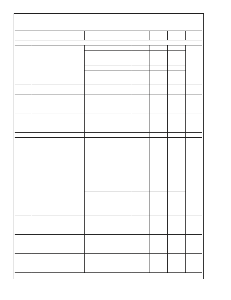
Electrical Characteristics
(Note 2) (Continued)
Unless otherwise specified, all limits guaranteed for T
J
= 25°C, V
S
=
±
5V, A
V(MAX)
= 10, V
CM
= 0V, R
F
= 1k
, R
G
= 174
, V
IN-
_DIFF
=
±
0.1V, R
L
= 100
, V
G
= +1V. Boldface limits apply at the temperature extremes.
Symbol
Parameter
Conditions
Min
(Note 6)
Typ
(Note 6)
Max
(Note 6)
Units
DC & Miscellaneous Performance
GACCU
Gain Accuracy (see Application
Notes)
V
G
=1.0V
+0.25
+0.9/-0.4
dB
0V
<
V
G
<
1V
±
0.3
+1.3/-1.5
-0.7V
<
V
G
<
1V
±
0.4
+4.4/-4.3
G Match
Gain Matching (see Application
Notes)
V
G
= 1.0
±
0.7
dB
0
<
V
G
<
1V
+1.7/-1.1
-0.7V
<
V
G
<
1V
+4.0/-4.7
K
Gain Multiplier (see Application
Notes)
1.58
1.58
1.72
1.87
1.91
V/V
V
CM
Input Voltage Range
Pin 3 & 6 Common Mode,
|CMRR|
>
50dB (Note 9)
±
2.0
±
1.80
±
2.2
V
V
IN_ DIFF
Differential Input Voltage
Across pins 3 & 6
±
0.34
±
0.28
±
0.37
V
I
RG MAX
R
G
Current
Pins 4 & 5
±
1.70
±
1.60
±
2.30
mA
I
BIAS
Bias Current
Pins 3 & 6 (Note 7)
11
18
20
µA
Pins 3 & 6 (Note 7),
V
S
=
±
2.5V
3
10
13
TC
BIAS
Bias Current Drift
Pin 3 & 6 (Note 8)
100
nA/°C
I
OFF
Offset Current
Pin 3 & 6
0.01
2.0
2.5
µA
TC I
OFF
Offset Current Drift
(Note 8)
5
nA/°C
R
IN
Input Resistance
Pin 3 & 6
750
k
C
IN
Input Capacitance
Pin 3 & 6
5
pF
IV
G
V
G
Bias Current
Pin 2, V
G
= 1.4V(Note 7)
45
µA
TC IV
G
V
G
Bias Drift
Pin 2 (Note 8)
20
nA/°C
R V
G
V
G
Input Resistance
Pin 2
70
K
C V
G
V
G
Input Capacitance
Pin 2
1.3
pF
V
OUT
Output Voltage Range
R
L
= 100
±
3.00
±
2.97
±
3.20
V
R
L
Open
±
3.95
±
3.90
±
4.05
R
OUT
Output Impedance
DC
0.1
I
OUT
Output Current
V
OUT
±
4V from Rails
±
75
±
70
±
90
mA
V
O
OFFSET
Output Offset Voltage
-1V
<
V
G
<
1V
±
80
±
350
±
380
mV
+PSRR
+Power Supply Rejection Ratio
(see (Note 10))
Input Referred, 1V change,
V
G
= 1.4V
-80
-58
-56
dB
-PSRR
-Power Supply Rejection Ratio
(see (Note 10))
Input Referred, 1V change,
V
G
= 1.4V
-67
-57
-51
dB
CMRR
Common Mode Rejection Ratio
(see (Note 9))
Input Referred, V
G
= 1V
-1.8V
<
V
CM
<
1.8V
-67
dB
I
S
Supply Current
R
L
= Open
37
50
53
mA
R
L
= Open, V
S
=
±
2.5V
12
20
23
LMH6503
www.national.com
3
Electrical Characteristics
(Note 2) (Continued)
Note 1: Absolute Maximum Ratings indicate limits beyond which damage to the device may occur. Operating Ratings indicate conditions for which the device is
intended to be functional, but specific performance is not guaranteed. For guaranteed specifications, see the Electrical Characteristics tables.
Note 2: Electrical Table values apply only for factory testing conditions at the temperature indicated. Factory testing conditions result in very limited self-heating of
the device such that T
J
= T
A
. No guarantee of parametric performance is indicated in the electrical tables under conditions of internal self-heating where T
J
>
T
A
.
Note 3: The maximum output current (I
OUT
) is determined by device power dissipation limitations or value specified, whichever is lower.
Note 4: Human body model: 1.5k
in series with 100pF. Machine model: 0 in series with 200pF.
Note 5: Slew Rate is the average of the rising and falling rates.
Note 6: Typical values represent the most likely parametric norm. Bold numbers refer to over temperature limits.
Note 7: Positive current correspondes to current flowing in the device.
Note 8: Drift determined by dividing the change in parameter distribution at temperature extremes by the total temperature change.
Note 9: CMRR definition: [|
V
OUT
/
V
CM
|/A
V
] with 0.1V differential input voltage.
V
OUT
is the change in output voltage with offset shift subtracted out.
Note 10: +PSRR definition: [|
V
OUT
/
V
+
| /A
V
], -PSRR definition: [|
V
OUT
/
V
-
| /A
V
] with 0.1V differential input voltage.
V
OUT
is the change in output voltage with
offset shift subtracted out.
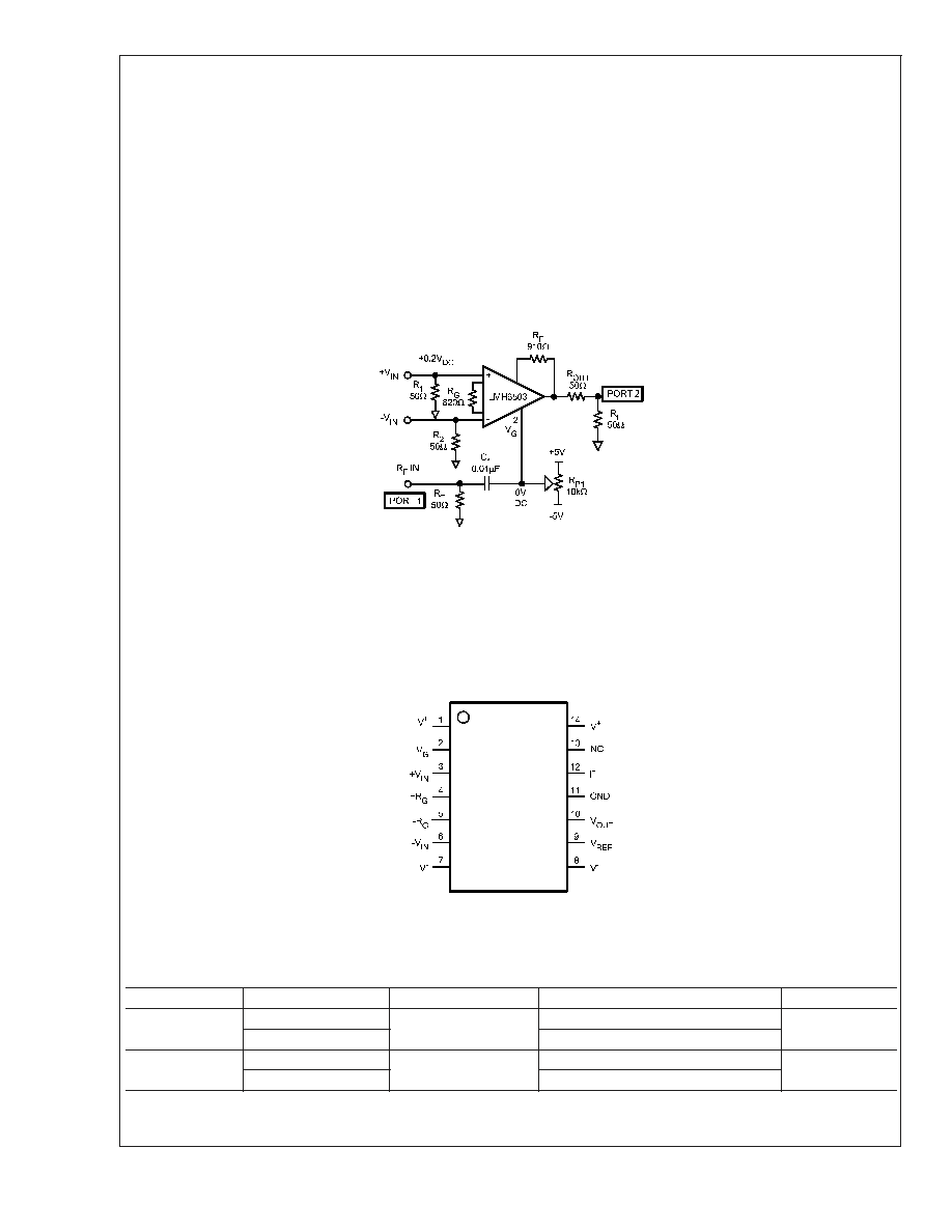
Note 11: Gain Control Frequency Response Schematic:
20073932
Note 12: Gain/Phase normalized to low frequency value at each A
V
.
Note 13: Flat Band Attenuation (Relative To Max Gain) Range Definition: Specified as the attenuation range from maximum which allows gain flatness specified
(either
±
0.2dB or
±
0.1dB), relative to A
VMAX
gain. For example, for f
<
30MHz, here are the Flat Band Attenuation ranges:
±
0.2dB:
10V/V down to 1V/V=20dB range
±
0.1dB:
10V/V down to 4.7V/V=6.5dB range
Connection Diagram
14-Pin SOIC/TSSOP
20073946
Top View
Ordering Information
Package
Part Number
Package Marking
Transport Media
NSC Drawing
14-pin SOIC
LMH6503MA
LMH6503MA
55 Units/Rail
M14A
LMH6503MAX
2.5k Units Tape and Reel
14-Pin TSSOP
LMH6503MT
LMH6503MT
94 Units/Rail
MTC14
LMH6503MTX
2.5k Units Tape and Reel
LMH6503
www.national.com
4
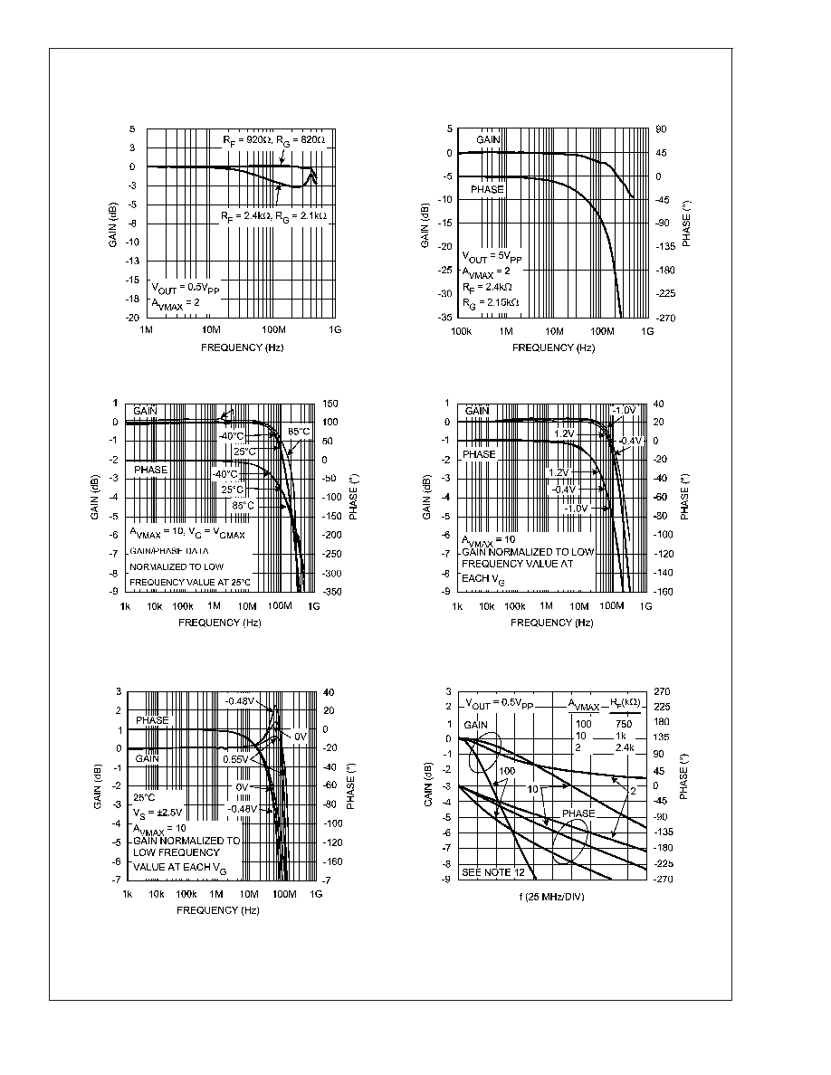
Typical Performance Charateristics
Unless otherwise specified: V
S
=
±
5V, 25°C, V
G
= V
G_MAX
, V
CM
= 0V, R
F
= 1k
, R
G
= 174
, both inputs terminated in 50, R
L
= 100
, Typical values, results referred to device output:
Small Signal Frequency Response (A
V
= 2)
Large Signal Frequency Response (A
V
= 2)
20073917
20073916
Frequency Response over Temperature (A
V
= 10)
Frequency Response for Various V
G
(A
VMAX
= 10)
20073919
20073920
Frequency Response for Various V
G
(A
VMAX
= 10)
(
±
2.5V)
Small Signal Frequency Response
20073930
20073914
LMH6503
www.national.com
5
Document Outline