
LMH6582/LMH6583
16x8 500 MHz Analog Crosspoint Switch, Gain of 1/
Gain of 2
General Description
The LMH
TM
family of products is joined by the LMH6582/
LMH6583, a high speed, non-blocking, analog, crosspoint
switch. The LMH6582 has a gain of 1 while the LMH6583
has a gain of two. The LMH6582/ LMH6583 is designed for
high speed, DC coupled, analog signals like high resolution
video (UXGA and higher). The LMH6582/ LMH6583 has 16
inputs and 8 outputs. The non-blocking architecture allows
an output to be connected to any input, including an input
that is already selected. With fully buffered inputs the
LMH6582/ LMH6583 can be impedance matched to nearly
any source impedance. The buffered outputs of the
LMH6582/ LMH6583 can drive up to two back terminated
video loads (75 Ohm load). The outputs and inputs also
feature high impedance inactive states allowing high perfor-
mance input and output expansion for array sizes such as 16
x 16 or 32 x 8 by combining two devices. The LMH6582/
LMH6583 is controlled with a 4 pin serial interface. Both
single serial mode and addressed chain modes are avail-
able.
The LMH6582/ LMH6583 comes in a 64�pin thermally en-
hanced TQFP package. It also has diagonally symmetrical
pin assignments to facilitate double sided board layouts and
easy pin connections for expansion. The package has an
exposed thermal pad on the bottom of the package.
Features
n
16 inputs and 8 outputs
n
64-pin exposed pad TQFP package
n
-3 dB bandwidth (V
OUT
= 0.5V
PP
)
500 MHz
n
-3 dB bandwidth (V
OUT
= 2V
PP
)
400 MHZ
n
Fast slew rate
3000 V/�s
n
Low crosstalk (10 MHz / 100 MHz)
-70 / -50 dBc
n
Easy to use serial programming
4 wire bus
n
Two programming modes
Serial & addressed modes
n
Symmetrical pinout facilitates expansion.
n
Output current
�
60 mA
n
Two gain options
A
V
= 1 or A
V
= 2
Applications
n
Studio monitoring/production video systems
n
Conference room mulitmedia video systems
n
KVM (keyboard video mouse) systems
n
Security/surveillance systems
n
Multi antenna diversity radio
n
Video test equipment
n
Medical imaging
n
Wide-band routers & switches
Connection Diagram
20150402
Block Diagram
20150411
TRI-STATE
�
is a registered trademark of National Semiconductor Corporation.
LMH
TM
is a trademark of National Semiconductor Corporation.
PRELIMINARY
April 2006
LMH6582/
LMH6583
16x8
500
MHz
Analog
Crosspoint
Switch,
Gain
of
1/Gain
of
2
� 2006 National Semiconductor Corporation
DS201504
www.national.com

Absolute Maximum Ratings
(Note 1)
If Military/Aerospace specified devices are required,
please contact the National Semiconductor Sales Office/
Distributors for availability and specifications.
V
S
�
6.2V
I
IN
(Input Pins)
�
20mA
I
OUT
(Note 3)
Input Voltage Range
V
-
to V
+
Maximum Junction Temperature
+150�C
Storage Temperature Range
-65�C to +150�C
Soldering Information
Infrared or Convection (20 sec.)
235�C
Wave Soldering (10 sec.)
260�C
ESD Tolerance (Note 5)
Human Body Model
2000V
Machine Model
200V
Operating Ratings
(Note 1)
Operating Temperature
-40�C to
+85�C
Supply Voltage Range
�
3V to
�
5.5V
Thermal Resistance
JA
JC
64�Pin Exposed Pad
TQFP
27�C/W
0.82�C/W
�
5V Electrical Characteristics
(Note 2)
Unless otherwise specified, typical conditions are: T
A
= 25�C, A
V
= +2, V
S
=
�
5V, R
L
= 100
; Boldface limits apply at the tem-
perature extremes.
Symbol
Parameter
Conditions
Min
(Note 8)
Typ
(Note 7)
Max
(Note 8)
Units
Frequency Domain Performance
SSBW
-3dB Bandwidth
V
OUT
=0.5V
PP
(Note 11)
500
MHz
LSBW
V
OUT
= 2V
PP
425
GF
0.1dB Gain Flatness
V
OUT
= 2V
PP
80
MHz
DG
Differential Gain
R
L
=150
, 3.58MHz/4.43MHz
%
DP
Differential Phase
R
L
= 150
, 3.58MHz/4.43MHz
deg
Time Domain Response
t
r
RiseTime
0.5V Step, 10% to 90%
ns
2V Step, 10% to 90%
1
ns
t
f
Fall Time
0.5V Step, 10% to 90%
ns
2V Step, 10% to 90%
1
ns
OS
Overshoot
2V Step
5
%
SR
Slew Rate
6V
PP
, 10% to 90% (Note 6)
3000
V/�s
t
s
Settling Time
4V Step, V
out
within 0.1%
ns
Distortion And Noise Response
HD2
2
nd
Harmonic Distortion
2V
PP
, 5MHz
dBc
HD3
3
rd
Harmonic Distortion
2V
PP
, 5MHz )
dBc
e
n
Input Referred Voltage Noise
>
1MHz
7
nV/
i
n
Input Referred Noise Current
>
1MHz
2
pA/
Switching Time
ns
XTLK
CrossTalk
All Hostile, f=100MHz
-50
dBc
ISOL
Off Isolation
f=100MHz
-65
dBc
Static, DC Performance
A
V
Gain
LMH6582
0.989
0.99
0.991
A
V
Gain
LMH6583
1.98
2.00
2.02
V
os
Output Offset Voltage
�
7
mV
TCV
os
Output Offset Voltage Average
Drift
(Note 10)
�V/�C
I
B
Input Bias Current
Non-Inverting (Note 9)
-7
�A
TCI
B
Input Bias Current Average Drift
Non-Inverting (Note 10)
nA/�C
V
O
Output Voltage Range
R
L
= 100
�
3.5
V
LMH6582/LMH6583
www.national.com
2

�
5V Electrical Characteristics
(Note 2) (Continued)
Unless otherwise specified, typical conditions are: T
A
= 25�C, A
V
= +2, V
S
=
�
5V, R
L
= 100
; Boldface limits apply at the tem-
perature extremes.
Symbol
Parameter
Conditions
Min
(Note 8)
Typ
(Note 7)
Max
(Note 8)
Units
PSRR
Power Supply Rejection Ratio
46
dB
I
S
Supply Current
R
L
=
110
mA
Tri State Supply Current
TRI pin
>
2.0V
25
mA
Miscellaneous Performance
R
IN
Input Resistance
Non-Inverting
M
C
IN
Input Capacitance
Non-Inverting
pF
R
O
Output Resistance
Closed Loop
m
CMVR
Input Common ModeVoltage
Range
�
3.0
V
I
O
Output Current
Sourcing, V
O
= 0 V
�
60
mA
Note 1: Absolute Maximum Ratings indicate limits beyond which damage to the device may occur. Operating Ratings indicate conditions for which the device is
intended to be functional, but specific performance is not guaranteed. For guaranteed specifications, see the Electrical Characteristics tables.
Note 2: Electrical Table typical values apply only for the conditions indicated. See Note 8 for limit specifications.
Note 3: The maximum output current (I
OUT
) is determined by device power dissipation limitations.
Note 4: The maximum power dissipation is a function of T
J(MAX)
,
JA
and T
A
. The maximum allowable power dissipation at any ambient temperature is P
D
=
(T
J(MAX)
-- T
A
)/
JA
. All numbers apply for package soldered directly into a 2 layer PC board with zero air flow.
Note 5: Human body model: 1.5k
in series with 100pF. Machine model: 0 in series with 200pF.
Note 6: Slew Rate is the average of the rising and falling edges.
Note 7: Typical numbers are the most likely parametric norm.
Note 8: Room Temperature limits are 100% production tested at 25�C. Factory testing conditions result in very limited self-heating of the device such that T
J
= T
A
.
Limits over the operating temperature range are guaranteed through correlation using Statistical Quality Control (SQC) methods.
Note 9: Negative input current implies current flowing out of the device.
Note 10: Drift determined by dividing the change in parameter at temperature extremes by the total temperature change.
Note 11: Parameter is guaranteed by design.
Ordering Information
Package
Part Number
Package Marking
Transport Media
NSC Drawing
64�Pin QFP
LMH6582YA
LMH6582YA
xx Units
VXE64A
LMH6583YA
LMH6583YA
xx Units
LMH6582/LMH6583
www.national.com
3

Application Section
INTRODUCTION
The LMH6582/ LMH6583 is a high speed, fully buffered, non
blocking, analog crosspoint switch. Having fully buffered
inputs allows the LMH6582/ LMH6583 to accept signals from
low or high impedance sources without the worry of loading
the signal source. The fully buffered outputs will drive 75 or
50 Ohm back terminated transmission lines with no external
components other than the termination resistor. The
LMH6582/ LMH6583 can have any input connected to any
(or all ) output(s). Conversely, a given output can have only
one associated input.
INPUT AND OUTPUT EXPANSION
The LMH6582/ LMH6583 has high impedance inactive
states for both inputs and outputs allowing maximum flexibil-
ity for Crosspoint expansion. In addition the LMH6582/
LMH6583 employs diagonal symmetry in pin assignments.
The diagonal symmetry makes it easy to use direct pin to pin
vias when the parts are mounted on opposite sides of a
board. As an example two LMH6582/ LMH6583 chips can be
combined on one board to form either an 16 x 16 crosspoint
or a 32x8 crosspoint. To make a 16 x 16 cross-point all 16
input pins would be tied together (Input 0 on side 1 to input
15 on side 2 and so on) while the 8 output pins on each chip
would be left separate. To make the 32 x 8 crosspoint, the 8
outputs would be tied together while all 32 inputs would
remain independent. In the 32 x 8 configuration it is impor-
tant not to have 2 connected outputs active at the same time.
With the 16 x 16 configuration, on the other hand, having two
connected inputs active is a valid state. Crosspoint expan-
sion as detailed above has the advantage that the signal
path has only one crosspoint in it at a time. Expansion
methods that have cascaded stages will suffer bandwidth
loss far greater than the small loading effect of parallel
expansion.
The LMH6582/ LMH6583 has fully buffered inputs and out-
puts. The inputs provide a low load, high impedance input
and ensure maximum performance from a variety of signal
sources. The fully buffered outputs will drive up to two back
terminated video loads. When disabled, the outputs are in a
high impedance state. When making thermal calculations
the output loading conditions will be a key consideration.
Please see the section on thermal management.
DRIVING CAPACITIVE LOADS
Capacitive output loading applications will benefit from the
use of a series output resistor R
OUT
. Capacitive loads of
5 to 120 pF are the most critical, causing ringing, frequency
response peaking and possible oscillation. The chart "Sug-
gested R
OUT
vs. Cap Load" gives a recommended value for
selecting a series output resistor for mitigating capacitive
loads. The values suggested in the charts are selected for
0.5 dB or less of peaking in the frequency response. This
gives a good compromise between settling time and band-
width. For applications where maximum frequency response
is needed and some peaking is tolerable, the value of R
OUT
can be reduced slightly from the recommended values.
When driving transmission lines the 50 or 75 Ohm matching
resistor makes the series output resistor unnecessary.
DIGITAL CONTROL
Block Diagram
20150411
The LMH6582/ LMH6583 has internal control registers that
store the programming states of the crosspoint switch. The
logic is two staged to allow for maximum programming flex-
ibility. The first stage of the control logic is tied directly to the
crosspoint switching matrix. This logic consists of one regis-
ter for each output that stores the on/off state and the
address of which input to connect to. These registers are not
directly accessible by the user. The second level of logic is
another bank of registers identical to the first, but set up as
shift registers. These registers are accessed by the user via
the serial input bus. As described further below, there are
two modes for programing the LMH6582, Serial Mode and
Addressed Mode.
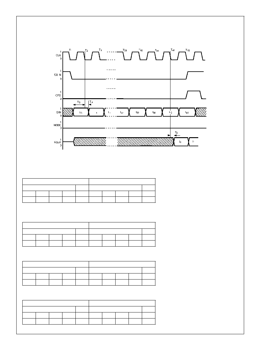
The LMH6582/ LMH6583is programmed via a serial input
bus with the support of 4 other digital control pins. The Serial
bus consists of a clock pin (CLK), a serial data in pin (DIN),
and a serial data out pin (DOUT). The serial bus is gated by
a chip select pin. The chip select pin is active low. While the
chip select pin is high all data on the serial input pin and
clock pins is ignored. When the chip select pin is brought low
the internal logic is set to begin receiving data by the first
positive transition (0 to 1) of the clock signal. The first data bit
is clocked in on the next negative transition. All input data is
read from the bus on the negative edge of the clock signal.
Once the last valid data has been clocked in, either the chip
select pin must go high or, the clock signal must stop.
Otherwise invalid data will be clocked into the chip. The data
clocked into the chip is not transferred to the crosspoint
matrix until the CFG pin is pulsed high. This is the case
regardless of the state of the Mode pin. The CFG pin is not
dependent on the state of the Chip select pin. If no new data
is clocked into the chip subsequent pulses on the CFG pin
will have no effect on device operation.
The programming format of the incoming serial data is se-
lected by the MODE pin. When the mode pin is HIGH the
crosspoint can be programmed one output at a time by
entering a string of data that contains the address of the
output that is going to be changed (Addressed Mode). When
the mode pin is LOW the crosspoint is in Serial Mode. In this
mode the crosspoint accepts a 40 bit array of data that
programs all of the outputs with the same data stream. In
both modes the data fed into the chip does not change the
LMH6582/LMH6583
www.national.com
4
Application Section
(Continued)
chip operation until the Configure pin is pulsed high. The
configure and mode pins are independent of the chip select
pin.
20150409
Timing Diagram for Serial Mode
Serial Mode Data Frame (First 2 Words)
Output 0
Output 1
Input Address
On=0
Input Address
On=0
LSB
MSB
Off=1
LSB
MSB
Off=1
0
1
2
3
4
5
6
7
8
9
Off = TRI-STATE
�
, Bit 0 is first bit clocked into device.
Serial Mode Data Frame (Continued)
Output 2
Output 3
Input Address
On=0
Input Address
On=0
LSB
MSB
Off=1
LSB
MSB
Off=1
10
11
12
13
14
15
16
17
18
19
Serial Mode Data Frame (Continued)
Output 4
Output 5
Input Address
On=0
Input Address
On=0
LSB
MSB
Off=1
LSB
MSB
Off=1
20
21
22
23
24
25
26
27
28
29
Serial Mode Data Frame (Last 2 Words)
Output 6
Output 7
Input Address
On=0
Input Address
On=0
LSB
MSB
Off=1
LSB
MSB
Off=1
30
31
32
33
34
35
36
37
38
39
Bit 39 is last bit clocked into device.
LMH6582/LMH6583
www.national.com
5