LMH6624/LMH6626
Single/Dual Ultra Low Noise Wideband Operational
Amplifier
General Description
The LMH6624/LMH6626 offer wide bandwidth (1.5GHz for
single, 1.3GHz for dual) with very low input noise (0.92nV/
, 2.3pA/
) and ultra low dc errors (100µV V
OS
,
±
0.1µV/∞C drift) providing very precise operational amplifiers
with wide dynamic range. This enables the user to achieve
closed-loop gains of greater than 10, in both inverting and
non-inverting configurations.
The LMH6624 (single) and LMH6626's (dual) traditional volt-
age feedback topology provide the following benefits: bal-
anced inputs, low offset voltage and offset current, very low
offset drift, 81dB open loop gain, 95dB common mode rejec-
tion ratio, and 88dB power supply rejection ratio.
The LMH6624/LMH6626 operate from
±
2.5V to
±
6V in
dual supply mode and from +5V to +12V in single supply
configuration.
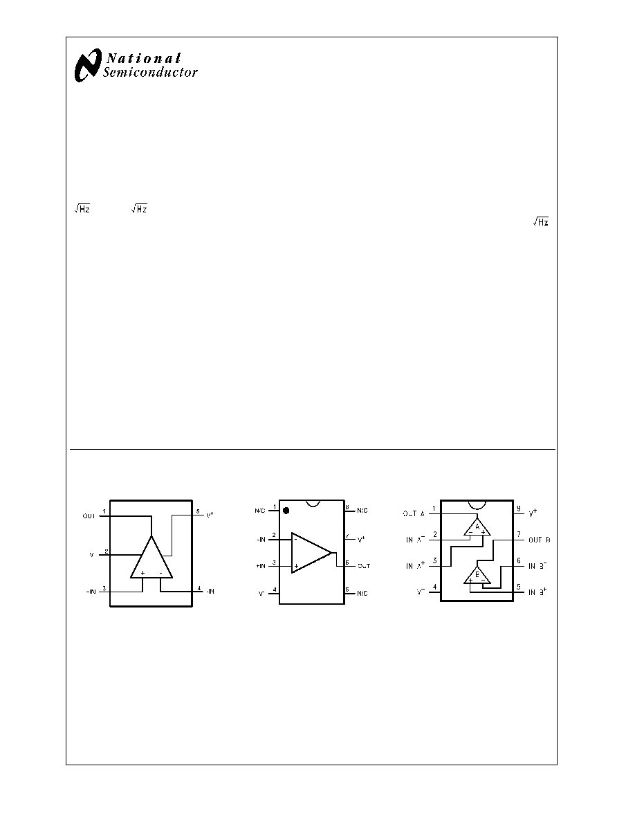
LMH6624 is offered in SOT23-5 and SOIC-8 packages.
The LMH6626 is offered in SOIC-8 and MSOP-8 packages.
Features
V
S
=
±
6V, T
A
= 25∞C, A
V
= 20, (Typical values unless
specified)
n
Gain bandwidth (LMH6624)
1.5GHz
n
Input voltage noise
0.92nV/
n
Input offset voltage (limit over temp)
700uV
n
Slew rate
350V/µs
n
Slew rate (A
V
= 10)
400V/µs
n
HD2
@
f = 10MHz, R
L
= 100
-63dBc
n
HD3
@
f = 10MHz, R
L
= 100
-80dBc
n
Supply voltage range (dual supply)
±
2.5V to
±
6V
n
Supply voltage range (single supply)
+5V to +12V
n
Improved replacement for the CLC425
(LMH6624)
n
Stable for closed loop |A
V
|
10
Applications
n
Instrumentation sense amplifiers
n
Ultrasound pre-amps
n
Magnetic tape & disk pre-amps
n
Wide band active filters
n
Professional Audio Systems
n
Opto-electronics
n
Medical diagnostic systems
Connection Diagrams
5-Pin SOT23
8-Pin SOIC
8-Pin SOIC/MSOP
20058951
Top View
20058952
Top View
20058961
Top View
September 2005
LMH6624/LMH6626
Single/Dual
Ultra
Low
Noise
W
ideband
Operational
Amplifier
© 2005 National Semiconductor Corporation
DS200589
www.national.com

Absolute Maximum Ratings
(Note 1)
If Military/Aerospace specified devices are required,
please contact the National Semiconductor Sales Office/
Distributors for availability and specifications.
ESD Tolerance
Human Body Model
2000V (Note 2)
Machine Model
200V (Note 9)
V
IN
Differential
±
1.2V
Supply Voltage (V
+
- V
-
)
13.2V
Voltage at Input pins
V
+
+0.5V, V
-
-0.5V
Soldering Information
Infrared or Convection (20 sec.)
235∞C
Wave Soldering (10 sec.)
260∞C
Storage Temperature Range
-65∞C to +150∞C
Junction Temperature (Note 3), (Note 4)
+150∞C
Operating Ratings
(Note 1)
Operating Temperature Range
(Note 3), (Note 4)
-40∞C to +125∞C
Package Thermal Resistance (
JA
)(Note 4)
SOIC-8
166∞C/W
SOT23≠5
265∞C/W
MSOP-8
235∞C/W
±
2.5V Electrical Characteristics
Unless otherwise specified, all limits guaranteed at T
A
= 25∞C, V
+
= 2.5V, V
-
= -2.5V, V
CM
= 0V, A
V
= +20, R
F
= 500
, R
L
=
100
. Boldface limits apply at the temperature extremes. See (Note 12).
Symbol
Parameter
Conditions
Min
(Note 6)
Typ
(Note 5)
Max
(Note 6)
Units
Dynamic Performance
f
CL
-3dB BW
V
O
= 400mV
PP
(LMH6624)
90
MHz
V
O
= 400mV
PP
(LMH6626)
80
SR
Slew Rate(Note 8)
V
O
= 2V
PP
, A
V
= +20 (LMH6624)
300
V/µs
V
O
= 2V
PP
, A
V
= +20 (LMH6626)
290
V
O
= 2V
PP
, A
V
= +10 (LMH6624)
360
V
O
= 2V
PP
, A
V
= +10 (LMH6626)
340
t
r
Rise Time
V
O
= 400mV Step, 10% to 90%
4.1
ns
t
f
Fall Time
V
O
= 400mV Step, 10% to 90%
4.1
ns
t
s
Settling Time 0.1%
V
O
= 2V
PP
(Step)
20
ns
Distortion and Noise Response
e
n
Input Referred Voltage Noise
f = 1MHz (LMH6624)
0.92
nV/
f = 1MHz (LMH6626)
1.0
i
n
Input Referred Current Noise
f = 1MHz (LMH6624)
2.3
pA/
f = 1MHz (LMH6626)
1.8
HD2
2
nd
Harmonic Distortion
f
C
= 10MHz, V
O
= 1V
PP
, R
L
100
-60
dBc
HD3
3
rd
Harmonic Distortion
f
C
= 10MHz, V
O
= 1V
PP
, R
L
100
-76
dBc
Input Characteristics
V
OS
Input Offset Voltage
V
CM
= 0V
-0.75
-0.95
-0.25
+0.75
+0.95
mV
Average Drift (Note 7)
V
CM
= 0V
±
0.25
µV/∞C
I
OS
Input Offset Current
V
CM
= 0V
-1.5
-2.0
-0.05
+1.5
+2.0
µA
Average Drift (Note 7)
V
CM
= 0V
2
nA/∞C
I
B
Input Bias Current
V
CM
= 0V
13
+20
+25
µA
Average Drift (Note 7)
V
CM
= 0V
12
nA/∞C
R
IN
Input Resistance (Note 10)
Common Mode
6.6
M
Differential Mode
4.6
k
C
IN
Input Capacitance (Note 10)
Common Mode
0.9
pF
Differential Mode
2.0
CMRR
Common Mode Rejection
Ratio
Input Referred,
dB
V
CM
= -0.5 to +1.9V
V
CM
= -0.5 to +1.75V
87
85
90
LMH6624/LMH6626
www.national.com
2
±
2.5V Electrical Characteristics
(Continued)
Unless otherwise specified, all limits guaranteed at T
A
= 25∞C, V
+
= 2.5V, V
-
= -2.5V, V
CM
= 0V, A
V
= +20, R
F
= 500
, R
L
=
100
. Boldface limits apply at the temperature extremes. See (Note 12).
Symbol
Parameter
Conditions
Min
(Note 6)
Typ
(Note 5)
Max
(Note 6)
Units
Transfer Characteristics
A
VOL
Large Signal Voltage Gain
(LMH6624)
R
L
= 100
, V
O
= -1V to +1V
75
70
79
dB
(LMH6626)
R
L
= 100
, V
O
= -1V to +1V
72
67
79
X
t
Crosstalk Rejection
f = 1MHz (LMH6626)
-75
dB
Output Characteristics
V
O
Output Swing
R
L
= 100
±
1.1
±
1.0
±
1.5
V
No Load
±
1.4
±
1.25
±
1.7
R
O
Output Impedance
f
100KHz
10
m
I
SC
Output Short Circuit Current
(LMH6624)
Sourcing to Ground
V
IN
= 200mV (Note 3), (Note 11)
90
75
145
mA
(LMH6624)
Sinking to Ground
V
IN
= -200mV (Note 3), (Note 11)
90
75
145
(LMH6626)
Sourcing to Ground
V
IN
= 200mV (Note 3),(Note 11)
60
50
120
(LMH6626)
Sinking to Ground
V
IN
= -200mV (Note 3),(Note 11)
60
50
120
I
OUT
Output Current
(LMH6624)
Sourcing, V
O
= +0.8V
Sinking, V
O
= -0.8V
100
mA
(LMH6626)
Sourcing, V
O
= +0.8V
Sinking, V
O
= -0.8V
75
Power Supply
PSRR
Power Supply Rejection Ratio
V
S
=
±
2.0V to
±
3.0V
82
80
90
dB
I
S
Supply Current (per channel)
No Load
11.4
16
18
mA
±
6V Electrical Characteristics
Unless otherwise specified, all limits guaranteed at T
A
= 25∞C, V
+
= 6V, V
-
= -6V, V
CM
= 0V, A
V
= +20, R
F
= 500
, R
L
=
100
. Boldface limits apply at the temperature extremes. See (Note 12).
Symbol
Parameter
Conditions
Min
(Note 6)
Typ
(Note 5)
Max
(Note 6)
Units
Dynamic Performance
f
CL
-3dB BW
V
O
= 400mV
PP
(LMH6624)
95
MHz
V
O
= 400mV
PP
(LMH6626)
85
SR
Slew Rate (Note 8)
V
O
= 2V
PP
, A
V
= +20 (LMH6624)
350
V/µs
V
O
= 2V
PP
, A
V
= +20 (LMH6626)
320
V
O
= 2V
PP
, A
V
= +10 (LMH6624)
400
V
O
= 2V
PP
, A
V
= +10 (LMH6626)
360
t
r
Rise Time
V
O
= 400mV Step, 10% to 90%
3.7
ns
LMH6624/LMH6626
www.national.com
3
±
6V Electrical Characteristics
(Continued)
Unless otherwise specified, all limits guaranteed at T
A
= 25∞C, V
+
= 6V, V
-
= -6V, V
CM
= 0V, A
V
= +20, R
F
= 500
, R
L
=
100
. Boldface limits apply at the temperature extremes. See (Note 12).
Symbol
Parameter
Conditions
Min
(Note 6)
Typ
(Note 5)
Max
(Note 6)
Units
t
f
Fall Time
V
O
= 400mV Step, 10% to 90%
3.7
ns
t
s
Settling Time 0.1%
V
O
= 2V
PP
(Step)
18
ns
Distortion and Noise Response
e
n
Input Referred Voltage Noise
f = 1MHz (LMH6624)
0.92
nV/
f = 1MHz (LMH6626)
1.0
i
n
Input Referred Current Noise
f = 1MHz (LMH6624)
2.3
pA/
f = 1MHz (LMH6626)
1.8
HD2
2
nd
Harmonic Distortion
f
C
= 10MHz, V
O
= 1V
PP
, R
L
100
-63
dBc
HD3
3
rd
Harmonic Distortion
f
C
= 10MHz, V
O
= 1V
PP
, R
L
100
-80
dBc
Input Characteristics
V
OS
Input Offset Voltage
V
CM
= 0V
-0.5
-0.7
±
0.10
+0.5
+0.7
mV
Average Drift (Note 7)
V
CM
= 0V
±
0.2
µV/∞C
I
OS
Input Offset Current Average
Drift (Note 7)
(LMH6624)
V
CM
= 0V
-1.1
-2.5
0.05
1.1
2.5
µA
(LMH6626)
V
CM
= 0V
-2.0
-2.5
0.1
2.0
2.5
V
CM
= 0V
0.7
nA/∞C
I
B
Input Bias Current
V
CM
= 0V
13
+20
+25
µA
Average Drift (Note 7)
V
CM
= 0V
12
nA/∞C
R
IN
Input Resistance (Note 10)
Common Mode
6.6
M
Differential Mode
4.6
k
C
IN
Input Capacitance (Note 10)
Common Mode
0.9
pF
Differential Mode
2.0
CMRR
Common Mode Rejection
Ratio
Input Referred,
dB
V
CM
= -4.5 to +5.25V
V
CM
= -4.5 to +5.0V
90
87
95
Transfer Characteristics
A
VOL
Large Signal Voltage Gain
(LMH6624)
R
L
= 100
, V
O
= -3V to +3V
77
72
81
dB
(LMH6626)
R
L
= 100
, V
O
= -3V to +3V
74
70
80
X
t
Crosstalk Rejection
f = 1MHz (LMH6626)
-75
dB
Output Characteristics
V
O
Output Swing
(LMH6624)
R
L
= 100
±
4.4
±
4.3
±
4.9
V
(LMH6624)
No Load
±
4.8
±
4.65
±
5.2
(LMH6626)
R
L
= 100
±
4.3
±
4.2
±
4.8
(LMH6626)
No Load
±
4.8
±
4.65
±
5.2
R
O
Output Impedance
f
100KHz
10
m
LMH6624/LMH6626
www.national.com
4

±
6V Electrical Characteristics
(Continued)
Unless otherwise specified, all limits guaranteed at T
A
= 25∞C, V
+
= 6V, V
-
= -6V, V
CM
= 0V, A
V
= +20, R
F
= 500
, R
L
=
100
. Boldface limits apply at the temperature extremes. See (Note 12).
Symbol
Parameter
Conditions
Min
(Note 6)
Typ
(Note 5)
Max
(Note 6)
Units
I
SC
Output Short Circuit Current
(LMH6624)
Sourcing to Ground
V
IN
= 200mV (Note 3), (Note 11)
100
85
156
mA
(LMH6624)
Sinking to Ground
V
IN
= -200mV (Note 3), (Note 11)
100
85
156
(LMH6626)
Sourcing to Ground
V
IN
= 200mV (Note 3), (Note 11)
65
55
120
(LMH6626)
Sinking to Ground
V
IN
= -200mV (Note 3), (Note 11)
65
55
120
I
OUT
Output Current
(LMH6624)
Sourcing, V
O
= +4.3V
Sinking, V
O
= -4.3V
100
mA
(LMH6626)
Sourcing, V
O
= +4.3V
Sinking, V
O
= -4.3V
80
Power Supply
PSRR
Power Supply Rejection Ratio
V
S
=
±
5.4V to
±
6.6V
82
80
88
dB
I
S
Supply Current (per channel)
No Load
12
16
18
mA
Note 1: Absolute maximum ratings indicate limits beyond which damage to the device may occur. Operating Ratings indicate conditions for which the device is
intended to be functional, but specific performance is not guaranteed. For guaranteed specifications and the test conditions, see the Electrical Characteristics.
Note 2: Human body model, 1.5k
in series with 100pF.
Note 3: Applies to both single-supply and split-supply operation. Continuous short circuit operation at elevated ambient temperature can result in exceeding the
maximum allowed junction temperature of 150∞C.
Note 4: The maximum power dissipation is a function of T
J(MAX)
,
JA
, and T
A
. The maximum allowable power dissipation at any ambient temperature is
P
D
= (T
J(MAX)
- T
A
)/
JA
. All numbers apply for packages soldered directly onto a PC board.
Note 5: Typical Values represent the most likely parametric norm.
Note 6: All limits are guaranteed by testing or statistical analysis.
Note 7: Average drift is determined by dividing the change in parameter at temperature extremes into the total temperature change.
Note 8: Slew rate is the slowest of the rising and falling slew rates.
Note 9: Machine Model, 0
in series with 200pF.
Note 10: Simulation results.
Note 11: Short circuit test is a momentary test. Output short circuit duration is 1.5ms.
Note 12: Electrical table values apply only for factory testing conditions at the temperature indicated. Factory testing conditions result in very limited self-heating of
the device such that T
J
= T
A
. No guarantee of parametric performance is indicated in the electrical tables under conditions of internal self-heating where T
J
>
T
A
.
Absolute maximum ratings indicate junction temperature limits beyond which the device may be permanently degraded, either mechanically or electrically.
Ordering Information
Package
Part Number
Package Marking
Transport Media
NSC Drawing
SOT23-5
LMH6624MF
A94A
1k Units Tape and Reel
MF05A
LMH6624MFX
3k Units Tape and Reel
SOIC-8
LMH6624MA
LMH6624MA
95 Units/Rail
M08A
LMH6624MAX
2.5k Units Tape and Reel
SOIC-8
LMH6626MA
LMH6626MA
95 Units/Rail
M08A
LMH6626MAX
2.5k Units Tape and Reel
MSOP-8
LMH6626MM
A98A
1k Units Tape and Reel
MUA08A
LMH6626MMX
3.5k Units Tape and Reel
LMH6624/LMH6626
www.national.com
5
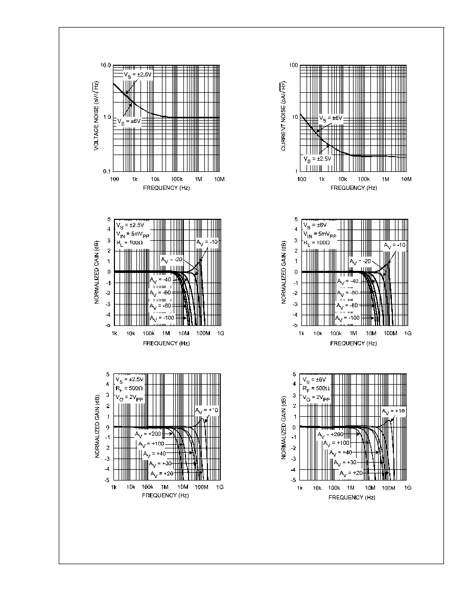
Typical Performance Characteristics
Voltage Noise vs. Frequency
Current Noise vs. Frequency
20058962
20058963
Inverting Frequency Response
Inverting Frequency Response
20058989
20058988
Non-Inverting Frequency Response
Non-Inverting Frequency Response
20058904
20058903
LMH6624/LMH6626
www.national.com
6

Typical Performance Characteristics
(Continued)
Open Loop Frequency Response Over Temperature
Open Loop Frequency Response Over Temperature
20058966
20058964
Frequency Response with Cap. Loading
Frequency Response with Cap. Loading
20058984
20058986
Frequency Response with Cap. Loading
Frequency Response with Cap. Loading
20058987
20058985
LMH6624/LMH6626
www.national.com
7

Typical Performance Characteristics
(Continued)
Non-Inverting Frequency Response Varying V
IN
Non-Inverting Frequency Response Varying V
IN
20058906
20058905
Non-Inverting Frequency Response Varying V
IN
(LMH6624)
Non-Inverting Frequency Response Varying V
IN
(LMH6626)
20058908
20058981
Non-Inverting Frequency Response Varying V
IN
(LMH6624)
Non-Inverting Frequency Response Varying V
IN
(LMH6626)
20058907
20058980
LMH6624/LMH6626
www.national.com
8

Typical Performance Characteristics
(Continued)
Sourcing Current vs. V
OUT
(LMH6624)
Sourcing Current vs. V
OUT
(LMH6626)
20058957
20058972
Sourcing Current vs. V
OUT
(LMH6624)
Sourcing Current vs. V
OUT
(LMH6626)
20058954
20058969
V
OS
vs. V
SUPPLY
(LMH6624)
V
OS
vs. V
SUPPLY
(LMH6626)
20058967
20058968
LMH6624/LMH6626
www.national.com
9

Typical Performance Characteristics
(Continued)
Sinking Current vs. V
OUT
(LMH6624)
Sinking Current vs. V
OUT
(LMH6626)
20058958
20058971
Sinking Current vs. V
OUT
(LMH6624)
Sinking Current vs. V
OUT
(LMH6626)
20058956
20058970
I
OS
vs. V
SUPPLY
Crosstalk Rejection vs. Frequency (LMH6626)
20058953
20058979
LMH6624/LMH6626
www.national.com
10
Typical Performance Characteristics
(Continued)
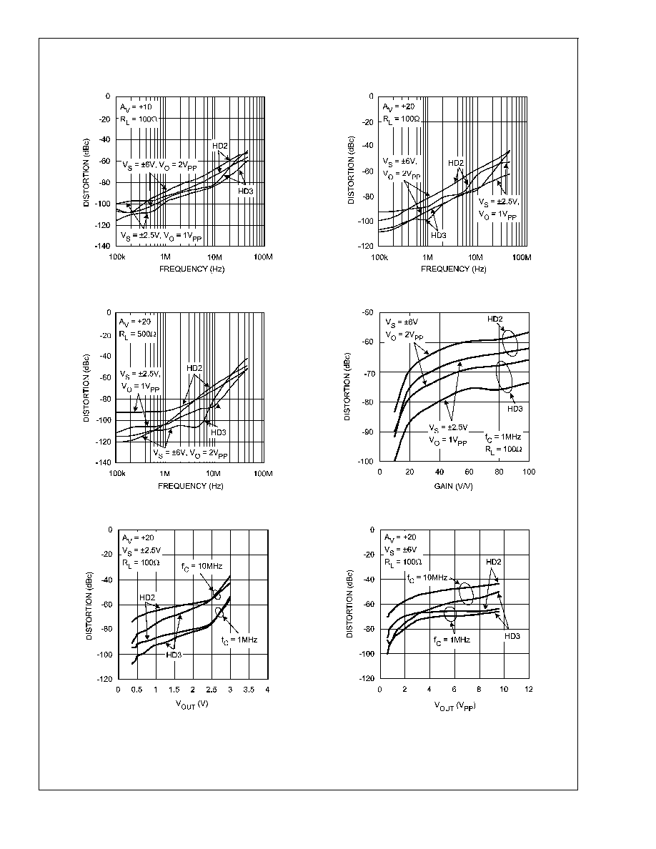
Distortion vs. Frequency
Distortion vs. Frequency
20058944
20058946
Distortion vs. Frequency
Distortion vs. Gain
20058945
20058978
Distortion vs. V
OUT
Peak to Peak
Distortion vs. V
OUT
Peak to Peak
20058943
20058977
LMH6624/LMH6626
www.national.com
11

Typical Performance Characteristics
(Continued)
Non-Inverting Large Signal Pulse Response
Non-Inverting Large Signal Pulse Response
20058973
20058974
Non-Inverting Small Signal Pulse Response
Non-Inverting Small Signal Pulse Response
20058975
20058976
PSRR vs. Frequency
PSRR vs. Frequency
20058948
20058949
LMH6624/LMH6626
www.national.com
12
Typical Performance Characteristics
(Continued)
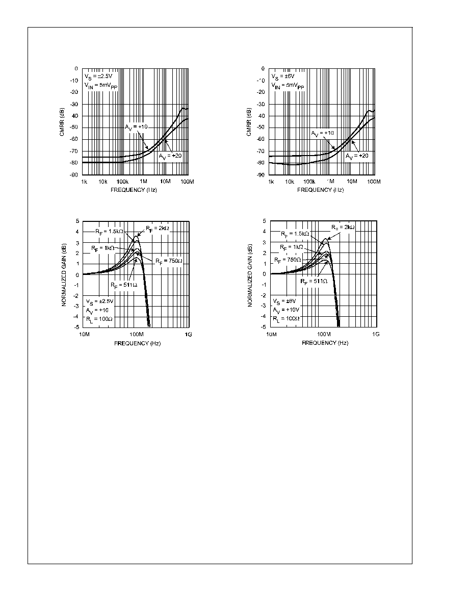
Input Referred CMRR vs. Frequency
Input Referred CMRR vs. Frequency
20058901
20058902
Amplifier Peaking with Varying R
F
Amplifier Peaking with Varying R
F
20058983
20058982
LMH6624/LMH6626
www.national.com
13
Application Section
INTRODUCTION
The LMH6624/LMH6626 are very wide gain bandwidth, ultra
low noise voltage feedback operational amplifiers. Their ex-
cellent performances enable applications such as medical
diagnostic ultrasound, magnetic tape & disk storage and
fiber-optics to achieve maximum high frequency signal-to-
noise ratios. The set of characteristic plots in the "Typical
Performance" section illustrates many of the performance
trade offs. The following discussion will enable the proper
selection of external components to achieve optimum sys-
tem performance.
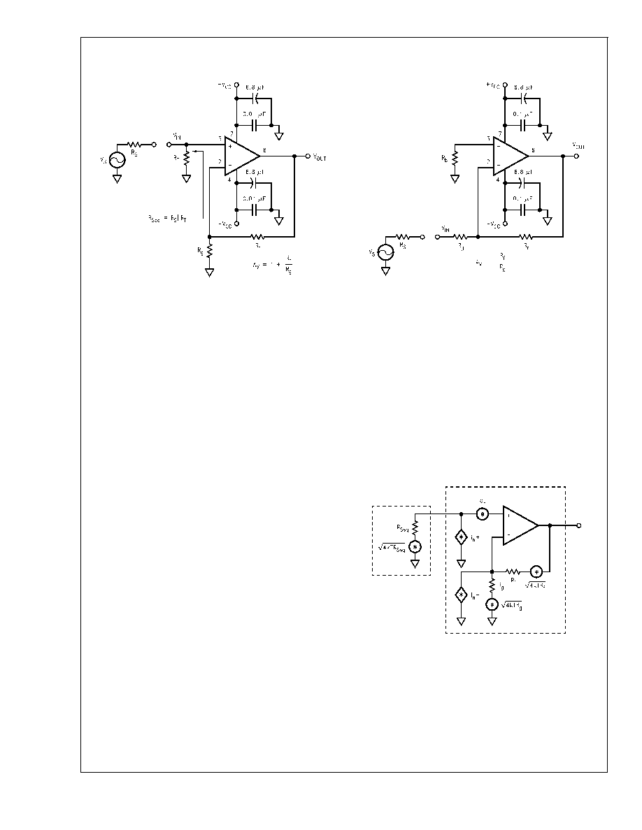
BIAS CURRENT CANCELLATION
To cancel the bias current errors of the non-inverting con-
figuration, the parallel combination of the gain setting (R
g
)
and feedback (R
f
) resistors should equal the equivalent
source resistance (R
seq
) as defined in Figure 1. Combining
this constraint with the non-inverting gain equation also seen
in Figure 1, allows both R
f
and R
g
to be determined explicitly
from the following equations:
R
f
= A
V
R
seq
and R
g
= R
f
/(A
V
-1)
When driven from a 0
source, such as the output of an op
amp, the non-inverting input of the LMH6624/LMH6626
should be isolated with at least a 25
series resistor.
As seen in Figure 2, bias current cancellation is accom-
plished for the inverting configuration by placing a resistor
(R
b
) on the non-inverting input equal in value to the resis-
tance seen by the inverting input (R
f
||(R
g
+R
s
)). R
b
should to
be no less than 25
for optimum LMH6624/LMH6626 per-
formance. A shunt capacitor can minimize the additional
noise of R
b
.
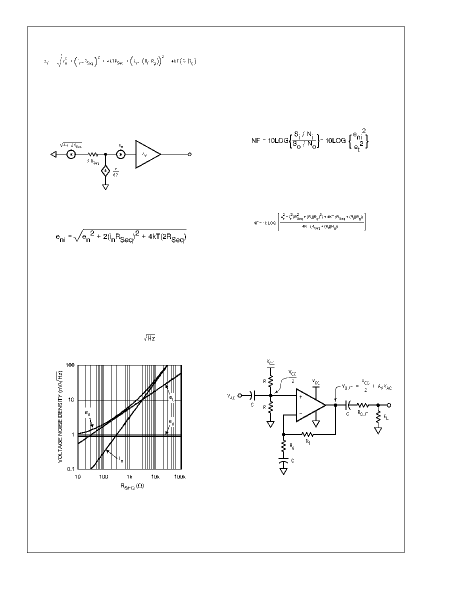
TOTAL INPUT NOISE vs. SOURCE RESISTANCE
To determine maximum signal-to-noise ratios from the
LMH6624/LMH6626, an understanding of the interaction be-
tween the amplifier's intrinsic noise sources and the noise
arising from its external resistors is necessary.
Figure 3 describes the noise model for the non-inverting
amplifier configuration showing all noise sources. In addition
to the intrinsic input voltage noise (e
n
) and current noise
(i
n
= i
n
+
= i
n
-
) source, there is also thermal voltage noise
(e
t
=
(4KTR)) associated with each of the external resistors.
Equation 1 provides the general form for total equivalent
input voltage noise density (e
ni
). Equation 2 is a simplifica-
tion of Equation 1 that assumes
20058918
FIGURE 1. Non-Inverting Amplifier Configuration
20058919
FIGURE 2. Inverting Amplifier Configuration
20058920
FIGURE 3. Non-Inverting Amplifier Noise Model
LMH6624/LMH6626
www.national.com
14
Application Section
(Continued)
(1)
R
f
||R
g
= R
seq
for bias current cancellation. Figure 4 illustrates
the equivalent noise model using this assumption. Figure 5
is a plot of e
ni
against equivalent source resistance (R
seq
)
with all of the contributing voltage noise source of Equation
2. This plot gives the expected e
ni
for a given (R
seq
) which
assumes R
f
||R
g
= R
seq
for bias current cancellation. The total
equivalent output voltage noise (e
no
) is e
ni
*A
V
.
(2)
As seen in Figure 5, e
ni
is dominated by the intrinsic voltage
noise (e
n
) of the amplifier for equivalent source resistances
below 33.5
. Between 33.5 and 6.43k, e
ni
is dominated
by the thermal noise (e
t
=
(4kT(2R
seq
)) of the external
resistor. Above 6.43k
, e
ni
is dominated by the amplifier's
current noise (i
n
=
(2) i
n
R
seq
). When R
seq
= 464
(ie.,
e
n
/
(2) i
n
) the contribution from voltage noise and current
noise of LMH6624/LMH6626 is equal.. For example, config-
ured with a gain of +20V/V giving a -3dB of 90MHz and
driven from R
seq
= 25
, the LMH6624 produces a total
equivalent input noise voltage (e
ni
x
1.57*90MHz) of
16.5µV
rms
.
If bias current cancellation is not a requirement, then R
f
||R
g
need not equal R
seq
. In this case, according to Equation 1,
R
f
||R
g
should be as low as possible to minimize noise.
Results similar to Equation 1 are obtained for the inverting
configuration of Figure 2 if R
seq
is replaced by R
b
and R
g
is
replaced by R
g
+ R
s
. With these substitutions, Equation 1 will
yield an e
ni
referred to the non-inverting input. Referring e
ni
to the inverting input is easily accomplished by multiplying
e
ni
by the ratio of non-inverting to inverting gains.
NOISE FIGURE
Noise Figure (NF) is a measure of the noise degradation
caused by an amplifier.
(3)
The Noise Figure formula is shown in Equation 3. The addi-
tion of a terminating resistor R
T
, reduces the external ther-
mal noise but increases the resulting NF. The NF is in-
creased because R
T
reduces the input signal amplitude thus
reducing the input SNR.
(4)
The noise figure is related to the equivalent source resis-
tance (R
seq
) and the parallel combination of R
f
and R
g
. To
minimize noise figure.
∑
Minimize R
f
||R
g
∑
Choose the Optimum R
S
(R
OPT
)
R
OPT
is the point at which the NF curve reaches a minimum
and is approximated by:
R
OPT
e
n
/i
n
SINGLE SUPPLY OPERATION
The LMH6624/LMH6626 can be operated with single power
supply as shown in Figure 6. Both the input and output are
capacitively coupled to set the DC operating point.
LOW NOISE TRANSIMPEDANCE AMPLIFIER
Figure 7 implements a low-noise transimpedance amplifier
commonly used with photo-diodes. The transimpedance
gain is set by R
f
. Equation 4 provides the total input current
20058921
FIGURE 4. Noise Model with R
f
||R
g
= R
seq
20058922
FIGURE 5. Voltage Noise Density vs. Source
Resistance
20058926
FIGURE 6. Single Supply Operation
LMH6624/LMH6626
www.national.com
15
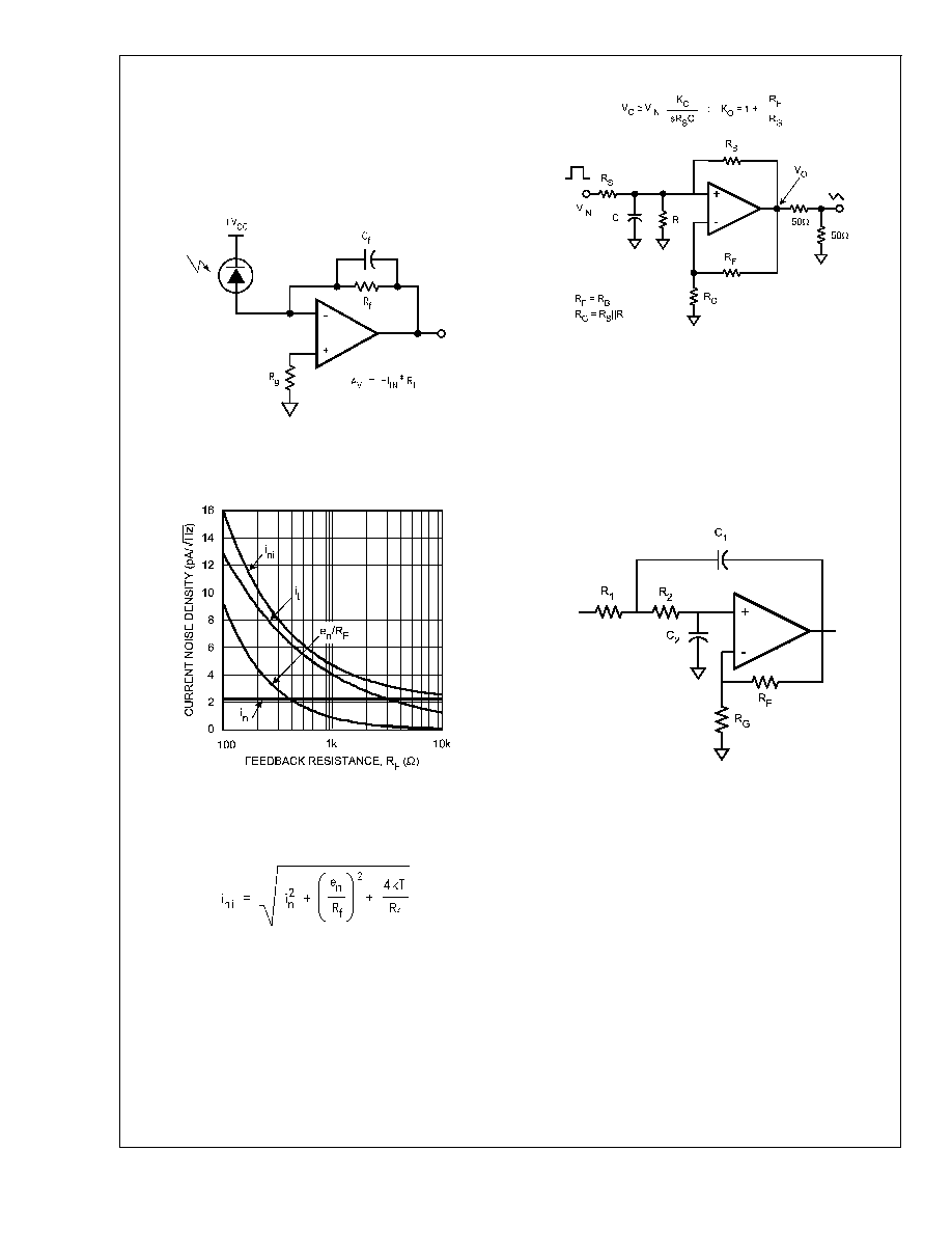
Application Section
(Continued)
noise density (i
ni
) equation for the basic transimpedance
configuration and is plotted against feedback resistance (R
f
)
showing all contributing noise sources in Figure 8. This plot
indicates the expected total equivalent input current noise
density (i
ni
) for a given feedback resistance (R
f
). The total
equivalent output voltage noise density (e
no
) is i
ni
*R
f
.
(5)
LOW NOISE INTEGRATOR
The LMH6624/LMH6626 implement a deBoo integrator
shown in Figure 9. Positive feedback maintains integration
linearity. The LMH6624/LMH6626's low input offset voltage
and matched inputs allow bias current cancellation and pro-
vide for very precise integration. Keeping R
G
and R
S
low
helps maintain dynamic stability.
HIGH-GAIN SALLEN-KEY ACTIVE FILTERS
The LMH6624/LMH6626 are well suited for high gain Sallen-
Key type of active filters. Figure 10 shows the 2
nd
order
Sallen-Key low pass filter topology. Using component predis-
tortion methods discussed in OA-21 enables the proper
selection of components for these high-frequency filters.
LOW NOISE MAGNETIC MEDIA EQUALIZER
The LMH6624/LMH6626 implement a high-performance low
noise equalizer for such application as magnetic tape chan-
nels as shown in Figure 11. The circuit combines an integra-
tor with a bandpass filter to produce the low noise equaliza-
tion. The circuit's simulated frequency response is illustrated
in Figure 12.
20058927
FIGURE 7. Transimpedance Amplifier Configuration
20058928
FIGURE 8. Current Noise Density vs. Feedback
Resistance
20058929
FIGURE 9. Low Noise Integrator
20058930
FIGURE 10. Sallen-Key Active Filter Topology
LMH6624/LMH6626
www.national.com
16
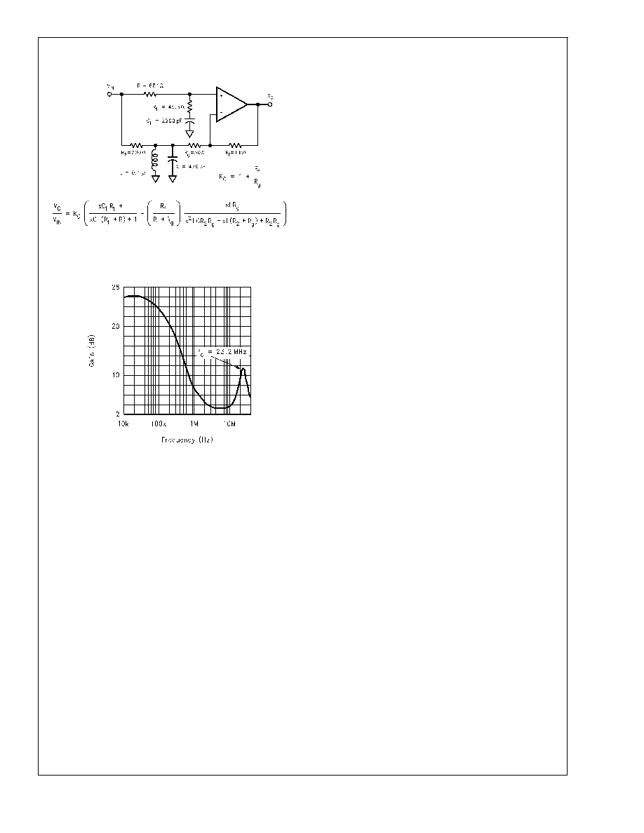
Application Section
(Continued)
LAYOUT CONSIDERATION
National Semiconductor suggests the copper patterns on the
evaluation boards listed below as a guide for high frequency
layout. These boards are also useful as an aid in device
testing and characterization. As is the case with all high-
speed amplifiers, accepted-practice RF design technique on
the PCB layout is mandatory. Generally, a good high fre-
quency layout exhibits a separation of power supply and
ground traces from the inverting input and output pins. Para-
sitic capacitances between these nodes and ground may
cause frequency response peaking and possible circuit os-
cillations (see Application Note OA-15 for more information).
Use high quality chip capacitors with values in the range of
1000pF to 0.1F for power supply bypassing. One terminal of
each chip capacitor is connected to the ground plane and the
other terminal is connected to a point that is as close as
possible to each supply pin as allowed by the manufacturer's
design rules. In addition, connect a tantalum capacitor with a
value between 4.7µF and 10µF in parallel with the chip
capacitor. Signal lines connecting the feedback and gain
resistors should be as short as possible to minimize induc-
tance and microstrip line effect. Place input and output ter-
mination resistors as close as possible to the input/output
pins. Traces greater than 1 inch in length should be imped-
ance matched to the corresponding load termination.
Symmetry between the positive and negative paths in the
layout of differential circuitry should be maintained to mini-
mize the imbalance of amplitude and phase of the differential
signal.
These free evaluation boards are shipped when a device
sample request is placed with National Semiconductor.
Component value selection is another important parameter
in working with high speed/high performance amplifiers.
Choosing external resistors that are large in value compared
to the value of other critical components will affect the closed
loop behavior of the stage because of the interaction of
these resistors with parasitic capacitances. These parasitic
capacitors could either be inherent to the device or be a
by-product of the board layout and component placement.
Moreover, a large resistor will also add more thermal noise to
the signal path. Either way, keeping the resistor values low
will diminish this interaction. On the other hand, choosing
very low value resistors could load down nodes and will
contribute to higher overall power dissipation and high dis-
tortion.
Device
Package
Evaluation Board Part
Number
LMH6624MF
SOT23≠5
CLC730216
LMH6624MA
SOIC-8
CLC730227
LMH6626MA
SOIC-8
CLC730036
LMH6626MM
MSOP-8
CLC730123
20058931
FIGURE 11. Noise Magnetic Media Equalizer
20058932
FIGURE 12. Equalizer Frequency Response
LMH6624/LMH6626
www.national.com
17
Physical Dimensions
inches (millimeters) unless otherwise noted
5-Pin SOT23
NS Package Number MF05A
8-Pin SOIC
NS Package Number M08A
LMH6624/LMH6626
www.national.com
18
Physical Dimensions
inches (millimeters) unless otherwise noted (Continued)
8-Pin MSOP
NS Package Number MUA08A
National does not assume any responsibility for use of any circuitry described, no circuit patent licenses are implied and National reserves
the right at any time without notice to change said circuitry and specifications.
For the most current product information visit us at www.national.com.
LIFE SUPPORT POLICY
NATIONAL'S PRODUCTS ARE NOT AUTHORIZED FOR USE AS CRITICAL COMPONENTS IN LIFE SUPPORT DEVICES OR SYSTEMS
WITHOUT THE EXPRESS WRITTEN APPROVAL OF THE PRESIDENT AND GENERAL COUNSEL OF NATIONAL SEMICONDUCTOR
CORPORATION. As used herein:
1. Life support devices or systems are devices or systems
which, (a) are intended for surgical implant into the body, or
(b) support or sustain life, and whose failure to perform when
properly used in accordance with instructions for use
provided in the labeling, can be reasonably expected to result
in a significant injury to the user.
2. A critical component is any component of a life support
device or system whose failure to perform can be reasonably
expected to cause the failure of the life support device or
system, or to affect its safety or effectiveness.
BANNED SUBSTANCE COMPLIANCE
National Semiconductor manufactures products and uses packing materials that meet the provisions of the Customer Products
Stewardship Specification (CSP-9-111C2) and the Banned Substances and Materials of Interest Specification (CSP-9-111S2) and contain
no ``Banned Substances'' as defined in CSP-9-111S2.
Leadfree products are RoHS compliant.
National Semiconductor
Americas Customer
Support Center
Email: new.feedback@nsc.com
Tel: 1-800-272-9959
National Semiconductor
Europe Customer Support Center
Fax: +49 (0) 180-530 85 86
Email: europe.support@nsc.com
Deutsch Tel: +49 (0) 69 9508 6208
English
Tel: +44 (0) 870 24 0 2171
FranÁais Tel: +33 (0) 1 41 91 8790
National Semiconductor
Asia Pacific Customer
Support Center
Email: ap.support@nsc.com
National Semiconductor
Japan Customer Support Center
Fax: 81-3-5639-7507
Email: jpn.feedback@nsc.com
Tel: 81-3-5639-7560
www.national.com
LMH6624/LMH6626
Single/Dual
Ultra
Low
Noise
W
ideband
Operational
Amplifier