 | ÐлекÑÑоннÑй компоненÑ: LMP7702MM | СкаÑаÑÑ:  PDF PDF  ZIP ZIP |
LMP7701/LMP7702/LMP7704 Precision, CMOS Input, RRIO, Wide Supply Range Amplifiers
LMP7701/LMP7702/LMP7704
Precision, CMOS Input, RRIO, Wide Supply Range
Amplifiers
General Description
The LMP7701/LMP7702/LMP7704 are single, dual, and
quad low offset voltage, rail-to-rail input and output precision
amplifiers each with CMOS input stage and wide supply
voltage range. The LMP7701/LMP7702/LMP7704 are part of
the LMP
TM
precision amplifier family and are ideal for sensor
interface and other instrumentation applications.
The guaranteed low offset voltage of less than
±
200 µV
along with the guaranteed low input bias current of less than
±
1 pA make the LMP7701 ideal for precision applications.
The LMP7701/LMP7702/LMP7704 are built utilizing VIP50
technology, which allows the combination of a CMOS input
stage and a 12V common mode and supply voltage range.
This makes the LMP7701/LMP7702/LMP7704 great choices
in many applications where conventional CMOS parts can-
not operate under the desired voltage conditions.
The LMP7701/LMP7702/LMP7704 have a rail-to-rail input
stage that significantly reduces the CMRR glitch commonly
associated with rail-to-rail input amplifiers. This is achieved
by trimming both sides of the complimentary input stage,
thereby reducing the difference between the NMOS and
PMOS offsets. The output of the LMP7701/LMP7702/
LMP7704 swings within 40 mV of either rail to maximize the
signal dynamic range in applications requiring low supply
voltage.
The LMP7701 is offered in the space saving 5-Pin SOT23
package, the LMP7702 is offered in the 8-Pin MSOP, and the
quad LMP7704 is offered in the 14-Pin TSSOP package.
These small packages are ideal solutions for area con-
strained PC boards and portable electronics.
Features
Unless otherwise noted, typical values at V
S
= 5V
n
Input offset voltage (LMP7701)
±
200 µV (max)
n
Input offset voltage (LMP7702/LMP7704)
±
220 µV (max)
n
Input bias current
±
200 fA
n
Input voltage noise
9 nV/
n
CMRR
130 dB
n
Open loop gain
130 dB
n
Temperature range
-40°C to 125°C
n
Unity gain bandwidth
2.5 MHz
n
Supply current (LMP7701)
715 µA
n
Supply current (LMP7702)
1.5 mA
n
Supply current (LMP7704)
2.9 mA
n
Supply voltage range
2.7V to 12V
n
Rail-to-rail input and output
Applications
n
High impedance sensor interface
n
Battery powered instrumentation
n
High gain amplifiers
n
DAC buffer
n
Instrumentation amplifier
n
Active filters
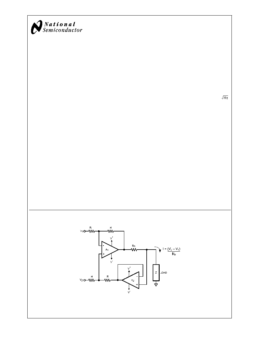
Typical Application
20127305
Precision Current Source
LMP
TM
is a trademark of National Semiconductor Corporation.
May 2006
LMP7701/LMP7702/LMP7704
Precision,
CMOS
Input,
RRIO,
W
ide
Supply
Range
Amplifiers
© 2006 National Semiconductor Corporation
DS201273
www.national.com
Absolute Maximum Ratings
(Note 1)
If Military/Aerospace specified devices are required,
please contact the National Semiconductor Sales Office/
Distributors for availability and specifications.
ESD Tolerance (Note 2)
Human Body Model
2000V
Machine Model
200V
V
IN
Differential
±
300 mV
Supply Voltage (V
S
= V
+
V
-
)
13.2V
Voltage at Input/Output Pins
V
+
+ 0.3V, V
-
- 0.3V
Input Current
10 mA
Storage Temperature Range
-65°C to +150°C
Junction Temperature (Note 3)
+150°C
Soldering Information
Infrared or Convection (20 sec)
235°C
Wave Soldering Lead Temp. (10
sec)
260°C
Operating Ratings
(Note 1)
Temperature Range (Note 3)
-40°C to +125°C
Supply Voltage (V
S
= V
+
V
-
)
2.7V to 12V
Package Thermal Resistance (
JA
(Note 3))
5-Pin SOT23
265°C/W
8-Pin MSOP
235°C/W
14-Pin TSSOP
122°C/W
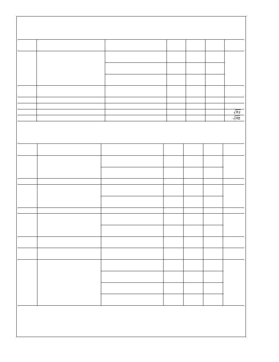
3V Electrical Characteristics
(Note 4)
Unless otherwise specified, all limits are guaranteed for T
A
= 25°C, V
+
= 3V, V
-
= 0V, V
CM
= V
+
/2, and R
L
>
10 k
to V
+
/2.
Boldface limits apply at the temperature extremes.
Symbol
Parameter
Conditions
Min
(Note 6)
Typ
(Note 5)
Max
(Note 6)
Units
V
OS
Input Offset Voltage
LMP7701
±
37
±
200
±
500
µV
LMP7702/LMP7704
±
56
±
220
±
520
TCV
OS
Input Offset Voltage Drift
(Note 7)
±
1
±
5
µV/°C
I
B
Input Bias Current
(Notes 7, 8)
-40°C
T
A
85°C
±
0.2
±
1
±
50
pA
(Notes 7, 8)
-40°C
T
A
125°C
±
0.2
±
1
±
400
I
OS
Input Offset Current
40
fA
CMRR
Common Mode Rejection Ratio
0V
V
CM
3V
LMP7701
86
80
130
dB
0V
V
CM
3V
LMP7702/LMP7704
84
78
130
PSRR
Power Supply Rejection Ratio
2.7V
V
+
12V, Vo = V
+
/2
86
82
98
dB
CMVR
Input Common-Mode Voltage Range
CMRR
80 dB
CMRR
77 dB
0.2
0.2
3.2
3.2
V
A
VOL
Large Signal Voltage Gain
R
L
= 2 k
(LMP7701)
V
O
= 0.3V to 2.7V
100
96
114
dB
R
L
= 2 k
(LMP7702/LMP7704)
V
O
= 0.3V to 2.7V
100
94
114
R
L
= 10 k
V
O
= 0.2V to 2.8V
100
96
124
LMP7701/LMP7702/LMP7704
www.national.com
2
3V Electrical Characteristics
(Note 4)
(Continued)
Unless otherwise specified, all limits are guaranteed for T
A
= 25°C, V
+
= 3V, V
-
= 0V, V
CM
= V
+
/2, and R
L
>
10 k
to V
+
/2.
Boldface limits apply at the temperature extremes.
Symbol
Parameter
Conditions
Min
(Note 6)
Typ
(Note 5)
Max
(Note 6)
Units
V
O
Output Swing High
R
L
= 2 k
to V
+
/2
LMP7701
40
80
120
mV
from V
+
R
L
= 2 k
to V
+
/2
LMP7702/LMP7704
40
80
150
R
L
= 10 k
to V
+
/2
LMP7701
30
40
60
R
L
= 10 k
to V
+
/2
LMP7702/LMP7704
35
50
100
Output Swing Low
R
L
= 2 k
to V
+
/2
LMP7701
40
60
80
mV
R
L
= 2 k
to V
+
/2
LMP7702/LMP7704
45
100
170
R
L
= 10 k
to V
+
/2
LMP7701
20
40
50
R
L
= 10 k
to V
+
/2
LMP7702/LMP7704
20
50
90
I
O
Output Short Circuit Current
(Notes 3, 9)
Sourcing V
O
= V
+
/2
V
IN
= 100 mV
25
15
42
mA
Sinking V
O
= V
+
/2
V
IN
= -100 mV (LMP7701)
25
20
42
Sinking V
O
= V
+
/2
V
IN
= -100 mV
(LMP7702/LMP7704)
25
15
42
I
S
Supply Current
LMP7701
0.670
1.0
1.2
mA
LMP7702
1.4
1.8
2.1
LMP7704
2.9
3.5
4.5
SR
Slew Rate (Note 10)
A
V
= +1, V
O
= 2 V
PP
10% to 90%
0.9
V/µs
GBW
Gain Bandwidth Product
2.5
MHz
THD+N
Total Harmonic Distortion + Noise
f = 1 kHz, A
V
= 1, R.
L
= 10 k
0.02
%
e
n
Input-Referred Voltage Noise
f = 1 kHz
9
nV/
i
n
Input-Referred Current Noise
f = 100 kHz
1
fA/
5V Electrical Characteristics
(Note 4)
Unless otherwise specified, all limits are guaranteed for T
A
= 25°C, V
+
= 5V, V
-
= 0V, V
CM
= V
+
/2, and R
L
>
10 k
to V
+
/2.
Boldface limits apply at the temperature extremes.
Symbol
Parameter
Conditions
Min
(Note 6)
Typ
(Note 5)
Max
(Note 6)
Units
V
OS
Input Offset Voltage
LMP7701
±
37
±
200
±
500
µV
LMP7702/LMP7704
±
32
±
220
±
520
TCV
OS
Input Offset Voltage Drift
(Note 7)
±
1
±
5
µV/°C
LMP7701/LMP7702/LMP7704
www.national.com
3
5V Electrical Characteristics
(Note 4)
(Continued)
Unless otherwise specified, all limits are guaranteed for T
A
= 25°C, V
+
= 5V, V
-
= 0V, V
CM
= V
+
/2, and R
L
>
10 k
to V
+
/2.
Boldface limits apply at the temperature extremes.
Symbol
Parameter
Conditions
Min
(Note 6)
Typ
(Note 5)
Max
(Note 6)
Units
I
B
Input Bias Current
(Notes 7, 8)
-40°C
T
A
85°C
±
0.2
±
1
±
50
pA
(Notes 7, 8)
-40°C
T
A
125°C
±
0.2
±
1
±
400
I
OS
Input Offset Current
40
fA
CMRR
Common Mode Rejection Ratio
0V
V
CM
5V
LMP7701
88
83
130
dB
0V
V
CM
5V
LMP7702/LMP7704
86
81
130
PSRR
Power Supply Rejection Ratio
2.7V
V
+
12V, V
O
= V
+
/2
86
82
100
dB
CMVR
Input Common-Mode Voltage Range
CMRR
80 dB
CMRR
78 dB
0.2
0.2
5.2
5.2
V
A
VOL
Large Signal Voltage Gain
R
L
= 2 k
(LMP7701)
V
O
= 0.3V to 4.7V
100
96
119
dB
R
L
= 2 k
(LMP7702/LMP7704)
V
O
= 0.3V to 4.7V
100
94
119
R
L
= 10 k
V
O
= 0.2V to 4.8V
100
96
130
V
O
Output Swing High
R
L
= 2 k
to V
+
/2
LMP7701
60
110
130
mV
from V
+
R
L
= 2 k
to V
+
/2
LMP7702/LMP7704
60
120
200
R
L
= 10 k
to V
+
/2
LMP7701
40
50
70
R
L
= 10 k
to V
+
/2
LMP7702/LMP7704
40
60
120
Output Swing Low
R
L
= 2 k
to V
+
/2
LMP7701
50
80
90
mV
R
L
= 2 k
to V
+
/2
LMP7702/LMP7704
50
120
190
R
L
= 10 k
to V
+
/2
LMP7701
30
40
50
R
L
= 10 k
to V
+
/2
LMP7702/LMP7704
30
50
100
I
O
Output Short Circuit Current
(Notes 3, 9)
Sourcing V
O
= V
+
/2
V
IN
= 100 mV (LMP7701)
40
28
66
mA
Sourcing V
O
= V
+
/2
V
IN
= 100 mV
(LMP7702/LMP7704)
38
25
66
Sinking V
O
= V
+
/2
V
IN
= -100 mV (LMP7701)
40
28
76
Sinking V
O
= V
+
/2
V
IN
= -100 mV
(LMP7702/LMP7704)
40
23
76
LMP7701/LMP7702/LMP7704
www.national.com
4
5V Electrical Characteristics
(Note 4)
(Continued)
Unless otherwise specified, all limits are guaranteed for T
A
= 25°C, V
+
= 5V, V
-
= 0V, V
CM
= V
+
/2, and R
L
>
10 k
to V
+
/2.
Boldface limits apply at the temperature extremes.
Symbol
Parameter
Conditions
Min
(Note 6)
Typ
(Note 5)
Max
(Note 6)
Units
I
S
Supply Current
LMP7701
0.715
1.0
1.2
mA
LMP7702
1.5
1.9
2.2
LMP7704
2.9
3.7
4.6
SR
Slew Rate (Note 10)
A
V
= +1, V
O
= 4 V
PP
10% to 90%
1.0
V/µs
GBW
Gain Bandwidth Product
2.5
MHz
THD+N
Total Harmonic Distortion + Noise
f = 1 kHz, A
V
= 1, R
L
= 10 k
0.02
%
e
n
Input-Referred Voltage Noise
f = 1 kHz
9
nV/
i
n
Input-Referred Current Noise
f = 100 kHz
1
fA/
±
5V Electrical Characteristics
(Note 4)
Unless otherwise specified, all limits are guaranteed for T
A
= 25°C, V
+
= 5V, V
-
= -5V, V
CM
= 0V, and R
L
>
10 k
to 0V.
Boldface limits apply at the temperature extremes.
Symbol
Parameter
Conditions
Min
(Note 6)
Typ
(Note 5)
Max
(Note 6)
Units
V
OS
Input Offset Voltage
LMP7701
±
37
±
200
±
500
µV
LMP7702/LMP7704
±
37
±
220
±
520
TCV
OS
Input Offset Voltage Drift
(Note 7)
±
1
±
5
µV/°C
I
B
Input Bias Current
(Notes 7, 8)
-40°C
T
A
85°C
±
0.2
1
±
50
pA
(Notes 7, 8)
-40°C
T
A
125°C
±
0.2
1
±
400
I
OS
Input Offset Current
40
fA
CMRR
Common Mode Rejection Ratio
-5V
V
CM
5V
LMP7701
92
88
138
dB
-5V
V
CM
5V
LMP7702/LMP7704
90
86
138
PSRR
Power Supply Rejection Ratio
2.7V
V
+
12V, V
O
= 0V
86
82
98
dB
CMVR
Input Common-Mode Voltage
Range
CMRR
80 dB
CMRR
78 dB
-5.2
-5.2
5.2
5.2
V
A
VOL
Large Signal Voltage Gain
R
L
= 2 k
(LMP7701)
V
O
= -4.7V to 4.7V
100
98
121
dB
R
L
= 2 k
(LMP7702/LMP7704)
V
O
= -4.7V to 4.7V
100
94
121
R
L
= 10 k
(LMP7701)
V
O
= -4.8V to 4.8V
100
98
134
R
L
= 10 k
(LMP7702/LMP7704)
V
O
= -4.8V to 4.8V
100
97
134
LMP7701/LMP7702/LMP7704
www.national.com
5
Document Outline