 | –≠–ª–µ–∫—Ç—Ä–æ–Ω–Ω—ã–π –∫–æ–º–ø–æ–Ω–µ–Ω—Ç: LMP8276 | –°–∫–∞—á–∞—Ç—å:  PDF PDF  ZIP ZIP |
LMP8271, LMP8276
High Common Mode, Gain of 20, Bidirectional Precision
Voltage Difference Amplifiers
General Description
The LMP
TM
8271, LMP8276 are fixed gain differential ampli-
fiers with a -2V to 27V input common mode voltage range
and a supply voltage range of 4.5V to 5.5V. The LMP8271,
LMP8276 are precision amplifiers which will detect, amplify
and filter small differential signals in the presence of high
common mode voltages. The gain is fixed at 20 and is
adequate to drive an ADC to full scale in most cases. This
fixed gain is achieved in two separate stages, a pre-amplifier
with gain of +10 and a second stage amplifier with a gain of
+2. The internal signal path is brought out on two pins that
provide a connection for a filter network.
The LMP8271, LMP8276 will function with reduced specifi-
cations over the extended common mode input voltage
range of -5 to 36 Volts. This feature makes the device
suitable for applications with load dump in automotive sys-
tems.
The midrail offset adjustment pin enables the user to utilize
this device for bidirectional current sensing. This is achieved
by adjusting an externally set voltage reference. Accurate
bidirectional load current measurements are achieved when
monitoring the output with respect to this reference voltage
Features
n
Bidirectional Current Sense Capability
n
Typical Values, TA = 25∞C
n
Input Offset Voltage
1mV max
n
TCVos (LMP8271)
15µV/∞C max
n
TCVos (LMP8276)
30µV/∞C max
n
CMRR
80dB Min
n
Extended CMVR
-5V to 36V
n
Output Voltage Swing
Rail to Rail
n
Bandwidth
80KHz
n
Operating Temperature Range (Ambient) -40∞C to 125∞C
n
Operating Temperature Range (bare die) -40∞C to 150∞C
n
Supply Voltage
4.5V to 5.5V
n
Supply Current
1mA
Applications
n
Fuel Injection Control
n
Low Side Driver Configuration Current Sensing
n
Power Management Systems
Typical Application
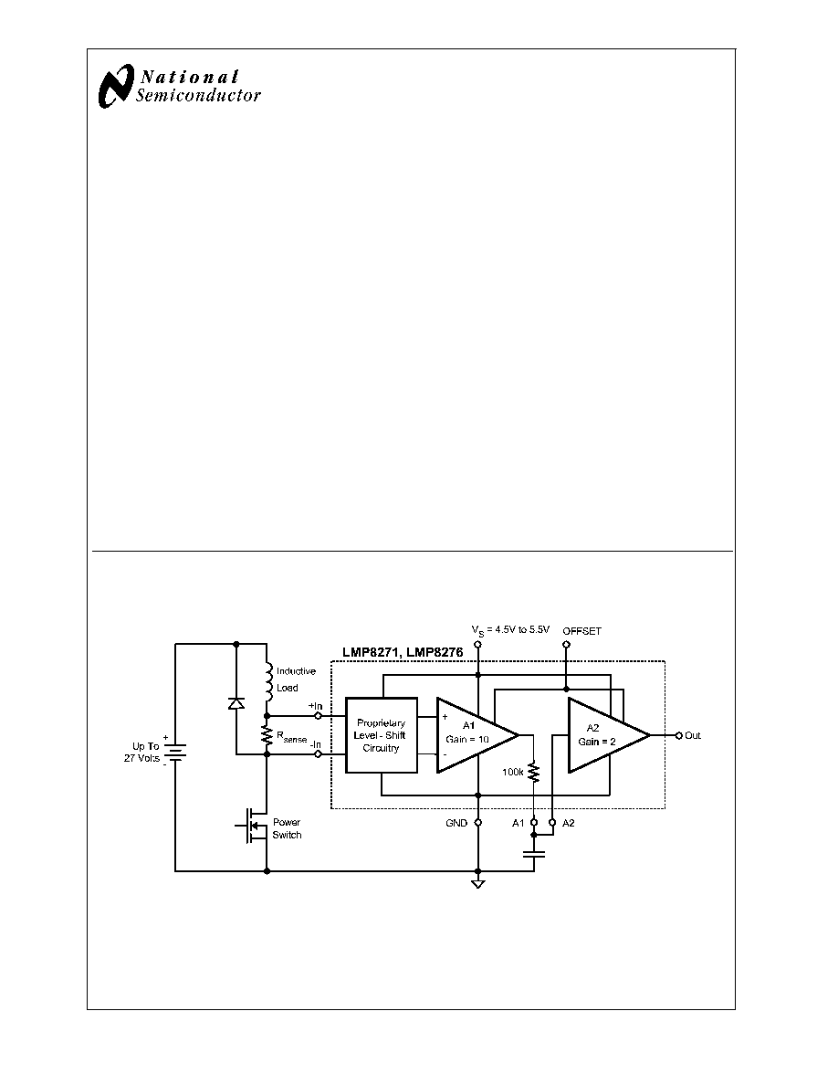
Typical Application: Low side Current Sensing
20130801
LMP
TM
is a trademark of National Semiconductor Corporation.
PRELIMINARY
January 2005
LMP8271,LMP8276
High
Common
Mode,
Gain
of
20,
Bidirectional
Precision
V
oltage
Difference
Amplifiers
© 2005 National Semiconductor Corporation
DS201308
www.national.com

Absolute Maximum Ratings
(Note 1)
If Military/Aerospace specified devices are required,
please contact the National Semiconductor Sales Office/
Distributors for availability and specifications.
ESD Tolerance (Note 2)
Human Body Model
For input pins only
±
4000V
For All other pins
±
2000V
Machine Model
200V
Supply Voltage (V
S
- GND)
5.75V
CMVR Continuous
-5 to 42 Volts
Transient (300 ms)
-TBD to 45 Volts
Storage Temperature Range
-65∞C to +150∞C
Junction Temperature (Note 3)
+150∞C max
Soldering Information
Infrared or Convection (20 sec)
235∞C
Wave Soldering Lead Temp. (10
sec)
260∞C
Operating Ratings
(Note 1)
Temperature Range (Note 3)
Packaged devices(Note 3)
-40∞C to +125∞C
Bare Die Junction Temperature(Note
3)
-40∞C to +150∞C
Supply Voltage (V
S
≠GND)
4.5V to 5.5V
Package Thermal Resistance (
JA
(Note 3))
8≠Pin SOIC
190∞C/W
5V Electrical Characteristics
(Note 7)
Unless otherwise specified, all limits guaranteed for T
A
= 25∞C, V
S
= 5V, GND= 0, -2V
V
CM
27V. Boldface limits apply at the
temperature extremes.
Symbol
Parameter
Conditions
Min
Typ
(Note
4)
Max
Units
V
OS
Input Offset Voltage
V
CM
= Vs/2
±
0.25
1.0
mV
TC V
OS
Input Offset Voltage Drift
LMP8271
±
6
±
15
µV/∞C
TC V
OS
Input Offset Voltage Drift
LMP8276
±
6
±
30
µV/∞C
A2 I
B
Input Bias Current of A2
(Note 5)
±
20
µA
I
S
Supply Current
0.6
TBD
1.0
1.2
TBD
mA
R
CM
Input impedance Common
Mode
160
200
240
K
R
DM
Input impedance Differential
Mode
320
400
480
K
CMVR
Input Common-Mode Voltage
Range
Continuous
-2
+27
V
ECMVR
Extended Common-Mode
Voltage Range
-5
36
V
DC
CMRR
DC Common Mode Rejection
Ratio
-2V
V
CM
27V
-5V
V
CM
36V
80
80
dB
AC
CMRR
AC Common Mode Rejection
Ratio
-2V
V
CM
27V
f = 1KHz
TBD
dB
-2V
V
CM
27V
f = 10KHz
TBD
PSRR
Power Supply Rejection Ratio
4.5V
V
S
5.5V
TBD
TBD
dB
R
F-INT
Filter Resistor
97
100
103
K
TCR
F-INT
Filter Resistor Drift
TBD
ppm/∞C
Midscale Offset Scaling
Accuracy (Pin 7)
1
%
A
V
Total Gain
20
V/V
Gain Error
±
1
%
Gain Drift
±
25
ppm/∞C
A1 V
OUT
A1 Output Voltage Swing
R
L
= 100K
on Output VOL
0.01
Volts
VOH
4.80
A2 V
OUT
A2 Output Voltage Swing
R
L
= 100K
on Output VOL
0.01
Volts
VOH
4.80
LMP8271,
LMP8276
High
Common
Mode,
Gain
of
20,
Bidirectional
Precision
V
oltage
Difference
Amplifier
www.national.com
2

5V Electrical Characteristics
(Note 7)
(Continued)
Unless otherwise specified, all limits guaranteed for T
A
= 25∞C, V
S
= 5V, GND= 0, -2V
V
CM
27V. Boldface limits apply at the
temperature extremes.
Symbol
Parameter
Conditions
Min
Typ
(Note
4)
Max
Units
SR
Slew Rate (Note 6)
0.7
V/µs
BW
Bandwidth
80
KHz
Noise
0.1Hz ro 10Hz
TBD
µVpp
Spectral Density
TBD
nV/
Hz
Note 1: Absolute Maximum Ratings indicate limits beyond which damage to the device may occur. Operating Ratings indicate conditions for which the device is
intended to be functional, but specific performance is not guaranteed. For guaranteed specifications and the test conditions, see the Electrical Characteristics Tables.
Note 2: Human body model, 1.5 k
in series with 100 pF. Machine model: 0 in series with 200 pF.
Note 3: The maximum power dissipation is a function of T
J(MAX)
,
JA
, and T
A
. The maximum allowable power dissipation at any ambient temperature is
P
D
= (T
J(MAX)
- T
A
)/
JA
. All numbers apply for packages soldered directly onto a PC board.
Note 4: Typical values represent the most likely parametric norm.
Note 5: Positive current corresponds to current flowing into the device.
Note 6: Slew rate is the average of the rising and falling slew rates.
Note 7: Electrical table values apply only for factory testing conditions at the temperature indicated. Factory testing conditions result in very limited self-heating of
the device.
Connection Diagram
8≠Pin SOIC
20130802
Top View
Application Note
The LMP8271, LMP8276 are single supply amplifier with a
fixed gain of 20 and an extended common mode voltage
range of -2V to 36V. The fixed gain is achieved in two
separate stages, a pre-amplifier with gain of +10 and a
second stage amplifier with gain of +2. A block diagram of
the LMP8271, LMP8276 is shown in Figure 1.
The overall offset of the LMP8271, LMP8276 is minimized by
trimming amplifier A1. This is done so that the output re-
ferred offset of A1 cancels the input referred offset of A2 or
10V
OS1
= -V
OS2
Because of this offset voltage relationship, the offset of each
individual amplifier stage maybe more than the limit speci-
fied for the overall system in the datasheet tables. Care must
be given when pin 3 and 4, A1 and A2, are connected to
each other. If the signal going from A1 to A2 is amplified or
attenuated (by use of amplifiers and resistors), the overall
LMP8271, LMP8276 offset will be affected as a result. Fil-
tering the signal between A1 and A2 or simply connecting the
two pins will not change the offset of the LMP8271,
LMP8276.
Referencing input referred offset voltages, the following re-
lationship holds:
If the signal on pin 3 is scaled, attenuated or amplified, by a
factor X then the offset of the overall system will become:
20130803
FIGURE 1.
LMP8271,
LMP8276
High
Common
Mode,
Gain
of
20,
Bidirectional
Precision
V
oltage
Difference
Amplifier
www.national.com
3
Application Note
(Continued)
This represents a value that the LMP8271 and LMP8276
have not been optimized and trimmed for and may very well
be above the limits indicated in the electrical characteristics
tables.
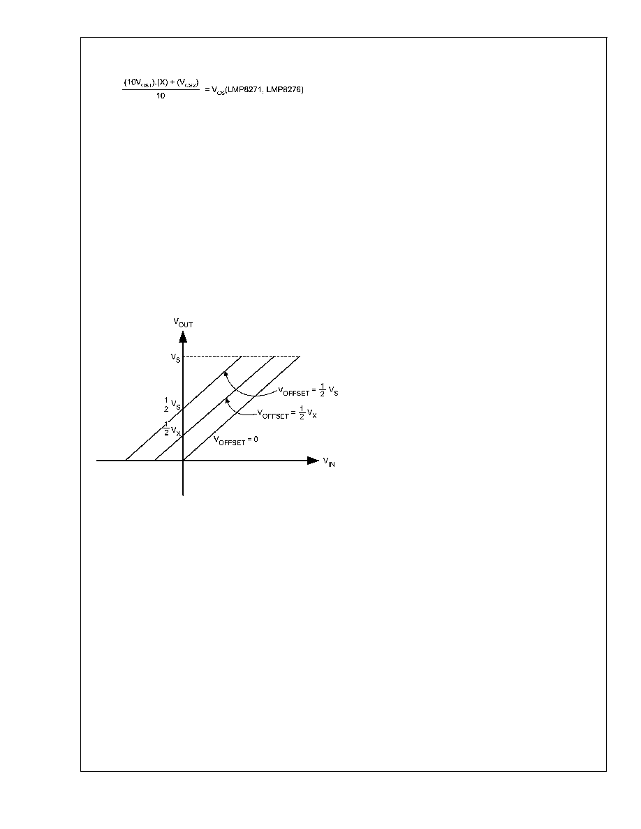
Midrail Offset Adjustment Pin
The external midrail offset adjustment pin enables the user
to utilize this device for bidirectional current sensing. If the
offset pin, pin 7, is connected to ground then the LMP8271,
LMP8276 are capable of sensing positive signals. When the
offset pin is connected to V
S
then 1/2V
S
is added to the
output and under this condition the amplifier can sense both
positive and negative signals. If this offset pin is connected
to any voltage between ground and V
S
, then the output is
increased by a voltage equal to half of that offset, e.g. If the
offset is connected to V
X
, then the output increases by
1/2V
X
. The following figure shows how this works:
Note that the offset pin, pin 7, needs to be connected at all
times. If the pin is left floating, the LMP8271 and LMP8276
will be operating in an undefined mode. Also pin 7 should be
driven from a low impedance source.
20130806
FIGURE 2.
LMP8271,
LMP8276
High
Common
Mode,
Gain
of
20,
Bidirectional
Precision
V
oltage
Difference
Amplifier
www.national.com
4

Notes
National does not assume any responsibility for use of any circuitry described, no circuit patent licenses are implied and National reserves
the right at any time without notice to change said circuitry and specifications.
For the most current product information visit us at www.national.com.
LIFE SUPPORT POLICY
NATIONAL'S PRODUCTS ARE NOT AUTHORIZED FOR USE AS CRITICAL COMPONENTS IN LIFE SUPPORT DEVICES OR SYSTEMS
WITHOUT THE EXPRESS WRITTEN APPROVAL OF THE PRESIDENT AND GENERAL COUNSEL OF NATIONAL SEMICONDUCTOR
CORPORATION. As used herein:
1. Life support devices or systems are devices or systems
which, (a) are intended for surgical implant into the body, or
(b) support or sustain life, and whose failure to perform when
properly used in accordance with instructions for use
provided in the labeling, can be reasonably expected to result
in a significant injury to the user.
2. A critical component is any component of a life support device
or system whose failure to perform can be reasonably
expected to cause the failure of the life support device or
system, or to affect its safety or effectiveness.
BANNED SUBSTANCE COMPLIANCE
National Semiconductor certifies that the products and packing materials meet the provisions of the Customer Products Stewardship
Specification (CSP-9-111C2) and the Banned Substances and Materials of Interest Specification (CSP-9-111S2) and contain no ``Banned
Substances'' as defined in CSP-9-111S2.
National Semiconductor
Americas Customer
Support Center
Email: new.feedback@nsc.com
Tel: 1-800-272-9959
National Semiconductor
Europe Customer Support Center
Fax: +49 (0) 180-530 85 86
Email: europe.support@nsc.com
Deutsch Tel: +49 (0) 69 9508 6208
English
Tel: +44 (0) 870 24 0 2171
FranÁais Tel: +33 (0) 1 41 91 8790
National Semiconductor
Asia Pacific Customer
Support Center
Email: ap.support@nsc.com
National Semiconductor
Japan Customer Support Center
Fax: 81-3-5639-7507
Email: jpn.feedback@nsc.com
Tel: 81-3-5639-7560
www.national.com
LMP8271,LMP8276
High
Common
Mode,
Gain
of
20,
Bidirectional
Precision
V
oltage
Difference
Amplifiers