LMP8276 High Common Mode, Gain of 20, Bidirectional Precision Voltage Difference Amplifier
LMP8276
High Common Mode, Gain of 20, Bidirectional Precision
Voltage Difference Amplifier
General Description
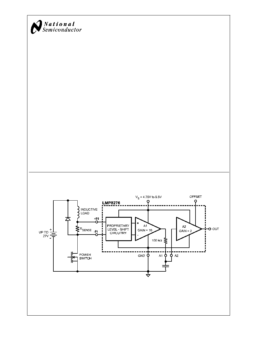
The LMP8276 is a fixed gain differential amplifier with a -2V
to 27V input common mode voltage range and a supply
voltage range of 4.75V to 5.5V. The LMP8276 is part of the
LMP
TM
precision amplifier family which will detect, amplify
and filter small differential signals in the presence of high
common mode voltages. The gain is fixed at 20 and is
adequate to drive an ADC to full scale in most cases. This
fixed gain is achieved in two separate stages, a preamplifier
with gain of +10 and a second stage amplifier with a gain of
+2. The internal signal path is brought out on two pins that
provide a connection for a filter network.
The LMP8276 will operate with reduced specifications over
the extended common mode input voltage range of -2V to
36V. This feature makes the device suitable for applications
with load dump in automotive systems.
The mid-rail offset adjustment pin enables the user to utilize
this device for bidirectional current sensing. This is achieved
by adjusting an externally set voltage reference. Accurate
bidirectional load current measurements are achieved when
monitoring the output with respect to this reference voltage.
Features
Typical Values, T
A
= 25°C
n
Bidirectional current sense capability
n
Input offset Voltage
±
2 mV max
n
TCVos
±
30 µV/°C max
n
CMRR
80 dB min
n
Extended CMVR
-2V to 36V
n
Output voltage swing
Rail-to-rail
n
Bandwidth
80 kHz
n
Operating temperature range (ambient)
-40°C to 125°C
n
Supply voltage
4.75V to 5.5V
n
Supply current
1 mA
Applications
n
Fuel injection control
n
High and low side driver configuration current sensing
n
Power management systems
Typical Application
Low Side Current Sensing
20130801
LMP
TM
is a trademark of National Semiconductor Corporation.
November 2005
LMP8276
High
Common
Mode,
Gain
of
20,
Bidirectional
Precision
V
oltage
Difference
Amplifier
© 2005 National Semiconductor Corporation
DS201308
www.national.com
Absolute Maximum Ratings
(Note 1)
If Military/Aerospace specified devices are required,
please contact the National Semiconductor Sales Office/
Distributors for availability and specifications.
ESD Tolerance (Note 2)
Human Body Model
For input pins only
±
4000V
For All other pins
±
2000V
Machine Model
200V
Supply Voltage (V
S
- GND)
5.75V
Voltage on +IN and -IN
-5V to 42V
Transient (400 ms)
-7V to 45V
Storage Temperature Range
-65°C to +150°C
Junction Temperature (Note 3)
+150°C max
Soldering Information
Infrared or Convection (20 sec)
235°C
Wave Soldering Lead Temp. (10 sec)
260°C
Operating Ratings
(Note 1)
Temperature Range
Packaged Devices (Note 3)
-40°C to +125°C
Supply Voltage (V
S
GND)
4.75V to 5.5V
Package Thermal Resistance (
JA
(Note 3))
8-Pin SOIC
190°C/W
5V Electrical Characteristics
(Note 4)
Unless otherwise specified, all limits are guaranteed for T
A
= 25°C, V
S
= 5V, GND = 0, -2V
V
CM
27V, R
L
= Open. Boldface
limits apply at the temperature extremes.
Symbol
Parameter
Conditions
Min
Typ
(Note 5)
Max
Units
V
OS
Input Offset Voltage
V
CM
= V
S
/2
±
0.25
±
2.0
mV
TC V
OS
Input Offset Voltage Drift
V
CM
= V
S
/2
25°C
T
A
125°C
±
20
±
30
µV/°C
-40°C
T
A
25°C
±
20
±
35
A2 I
B
Input Bias Current of A2
(Note 6)
±
20
nA
I
S
Supply Current
1.0
1.2
1.4
mA
R
CM
Input Impedance Common Mode
160
200
240
k
R
DM
Input Impedance Differential Mode
320
400
480
k
CMVR
Input Common-Mode Voltage
Range
-2
+27
V
ECMVR
Extended Common-Mode Voltage
Range
-2
36
V
DC
CMRR
DC Common Mode Rejection Ratio 0°C
T
A
125°C
-2V
V
CM
27V
-2V
V
CM
36V
80
60
103
dB
-40°C
T
A
0°C
-2V
V
CM
27V
-2V
V
CM
36V
77
60
AC
CMRR
AC Common Mode Rejection Ratio
(Note 7)
-2V
V
CM
27V
f = 1 kHz
80
dB
f = 10 kHz
78
PSRR
Power Supply Rejection Ratio
4.75V
V
S
5.5V
70
80
dB
R
F-INT
Filter Resistor
97
100
103
k
TCR
F-INT
Filter Resistor Drift
20
ppm/°C
Midscale Offset Scaling Accuracy
(Pin 7)
1
%
A
V
Total Gain
19.8
20
20.2
V/V
Gain Drift
±
25
ppm/°C
A
V1
A1 Gain
9.9
10
10.1
V/V
A
V2
A2 Gain
1.98
2
2.02
V/V
A1 V
OUT
A1 Output Voltage Swing
VOL
0.004
0.001
V
VOH
4.80
4.95
A2 V
OUT
A2 Output Voltage Swing
(Notes 8, 9)
R
L
= 100 k
on Output VOL
0.007
0.02
V
VOH
4.80
4.99
R
L
= 10 k
on Output VOL
0.03
V
VOH
4.95
SR
Slew Rate (Note 10)
0.7
V/µs
LMP8276
www.national.com
2
5V Electrical Characteristics
(Note 4)
(Continued)
Unless otherwise specified, all limits are guaranteed for T
A
= 25°C, V
S
= 5V, GND = 0, -2V
V
CM
27V, R
L
= Open. Boldface
limits apply at the temperature extremes.
Symbol
Parameter
Conditions
Min
Typ
(Note 5)
Max
Units
BW
Bandwidth
80
kHz
Noise
0.1 Hz to 10 Hz
5.7
µV
PP
Spectral Density
f = 1kHz
452
nV/
Note 1: Absolute Maximum Ratings indicate limits beyond which damage to the device may occur. Operating Ratings indicate conditions for which the device is
intended to be functional, but specific performance is not guaranteed. For guaranteed specifications and the test conditions, see the Electrical Characteristics Tables.
Note 2: Human Body Model is 1.5 k
in series with 100 pF. Machine Model is 0 in series with 200 pF.
Note 3: The maximum power dissipation is a function of T
J(MAX)
,
JA
, and T
A
. The maximum allowable power dissipation at any ambient temperature is
P
D
= (T
J(MAX)
- T
A
)/
JA
. All numbers apply for packages soldered directly onto a PC board.
Note 4: Electrical table values apply only for factory testing conditions at the temperature indicated. Factory testing conditions result in very limited self-heating of
the device.
Note 5: Typical values represent the parametric norm at the time of characterization.
Note 6: Positive current corresponds to current flowing into the device.
Note 7: AC Common Mode Signal is a 24 V
PP
sine-wave (0V to 24V) at the given frequency.
Note 8: For VOL, R
L
is connected to V
S
and for VOH, R
L
is connected to GND.
Note 9: For this test input is driven from A1 stage.
Note 10: Slew rate is the average of the rising and falling slew rates.
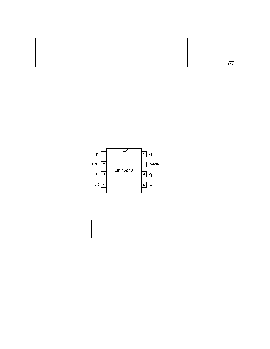
Connection Diagram
8-Pin SOIC
20130802
Top View
Ordering Information
Package
Part Number
Package Marking
Transport Media
NSC Drawing
8-Pin SOIC
LMP8276MA
LMP8276MA
95 Units/Rail
M08A
LMP8276MAX
2.5k Units Tape and Reel
LMP8276
www.national.com
3
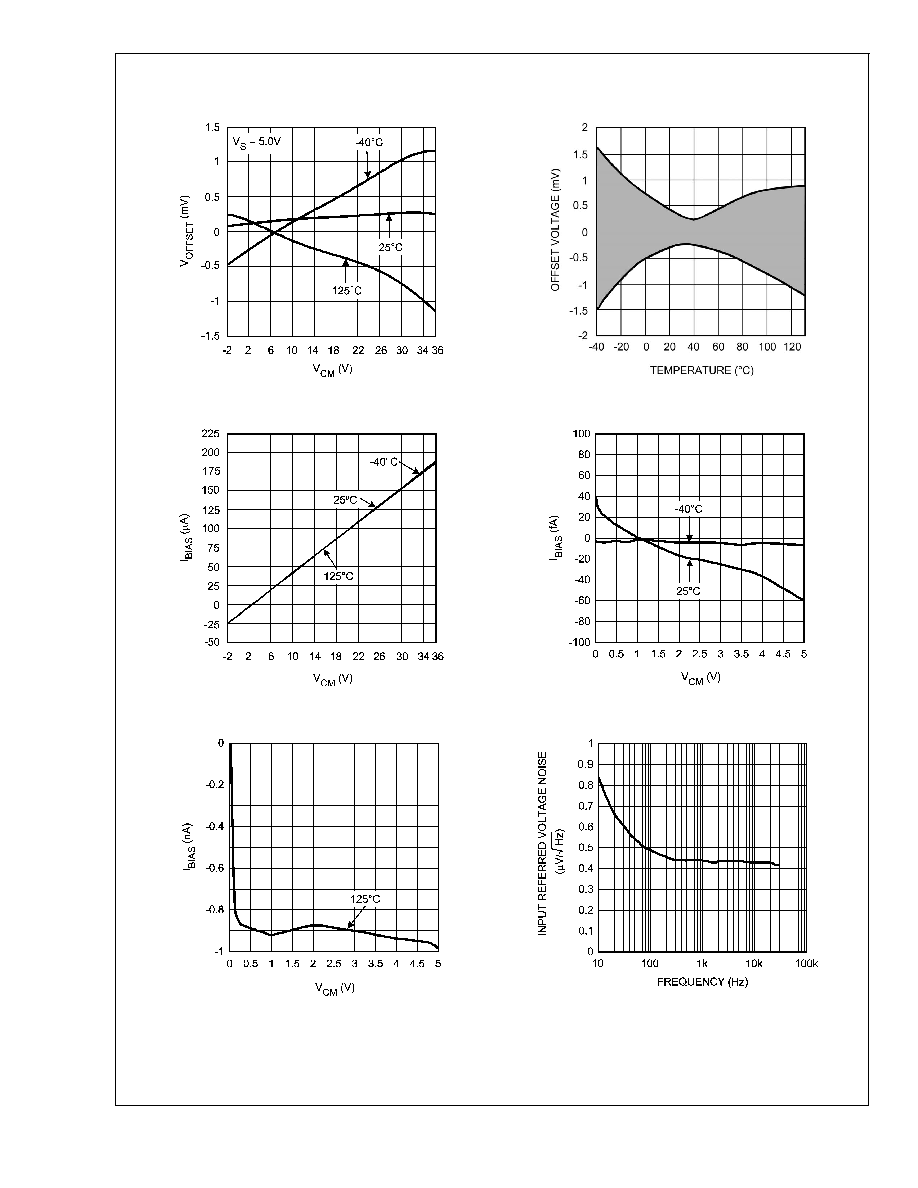
Typical Performance Characteristics
Unless otherwise specified: T
A
= 25°C, V
S
= 5V, V
CM
= V
S
/2
V
OS
vs. V
CM
Over Temperature
Typical V
OS
vs. Temperature
20130815
20130821
Input Bias Current Over Temperature (A1 Inputs)
Input Bias Current Over Temperature (A2 Inputs)
20130819
20130818
Input Bias Current Over Temperature (A2 Inputs)
Input Referred Voltage Noise vs. Frequency
20130820
20130806
LMP8276
www.national.com
4
Typical Performance Characteristics
Unless otherwise specified: T
A
= 25°C, V
S
= 5V, V
CM
= V
S
/2
(Continued)
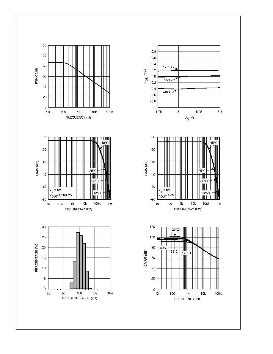
PSRR vs. Frequency
V
OS
vs. Supply Voltage
20130823
20130822
Gain vs. Frequency Over Temperature
Gain vs. Frequency Over Temperature
20130812
20130811
Filter Resistor
CMRR vs. Frequency
20130817
20130814
LMP8276
www.national.com
5
Document Outline