Äîêóìåíòàöèÿ è îïèñàíèÿ www.docs.chipfind.ru
LMS1585AEP/LMS1587EP
Enhanced Plastic 5A and 3A Low Dropout Fast
Response Regulators
General Description
The LMS1585AEP and LMS1587EP are low dropout posi-
tive regulators with output load current of 5A and 3A respec-
tively. Their low dropout voltage (1.2V) and fast transient
response make them an excellent solution for low voltage
microprocessor applications.
The LMS1585AEP/87EP are available in adjustable ver-
sions, which can set the output voltage with only two external
resistors. In addition, they are also available in 1.5V and
3.3V fixed voltage versions (Note 12).
The LMS1585AEP/87EP circuits include a zener trimmed
bandgap reference, current limiting and thermal shutdown.
The LMS1585AEP/87EP series are available in TO-220 and
TO-263 packages.
ENHANCED PLASTIC
·
Extended Temperature Performance of -40°C to 125°C
·
Baseline Control - Single Fab & Assembly Site
·
Process Change Notification (PCN)
·
Qualification & Reliability Data
·
Solder (PbSn) Lead Finish is standard
·
Enhanced Diminishing Manufacturing Sources (DMS)
Support
Features
n
Fast transient response
n
Available in Adjustable, 1.5V, and 3.3V versions
n
Current limiting and thermal protection
n
Line regulation
0.005% (typical)
n
Load regulation
0.05% (typical)
Applications
n
Low voltage logic supplies
n
Selected Military Applications
n
Selected Avionics Applications
Ordering Information
PART NUMBER
VID PART NUMBER
NS PACKAGE NUMBER (Note 3)
LMS1585AIS33EP
V62/04639-01
TS3B
LMS1585AISADJEP
V62/04639-02
TS3B
LMS1587ISXADJEP
V62/04639-03
TS3B
(Notes 1, 2)
TBD
TBD
Note 1: For the following (Enhanced Plastic) version, check for availability: LMS1585ACT3.3EP, LMS1585ACTADJEP, LMS1585AIT1.5EP,
LMS1585AIT3.3EP, LMS1585AITADJEP, LMS1585ACS1.5EP, LMS1585ACS3.3EP, LMS1585ACSADJEP, LMS1585AIS1.5EP, LMS1585ACSX33EP,
LMS1585CSXADJEP, LMS1585AISX15EP, LMS1585AISX33EP, LMS1585ASXADJEP, LMS1587CT1.5EP, LMS1587CT3.3EP, LMS1587CTADJEP,
LMS1587IT1.5EP, LMS1587IT3.3EP, LMS1587ITADJEP, LMS1587CS1.5EP, LMS1587CS3.3EP, LMS1587CSADJEP, LMS1587IS1.5EP, LMS1587IS3.3EP,
LMS1587ISADJEP, LMS1587CSX3.3EP, LMS1587CSXADJEP, LMS1587ISX1.5EP, LMS1587ISX3.3EP. Parts listed with an "X" are provided in Tape &
Reel and parts without an "X" are in Rails.
Note 2: FOR ADDITIONAL ORDERING AND PRODUCT INFORMATION, PLEASE VISIT THE ENHANCED PLASTIC WEB SITE AT: www.national.com/
mil
Note 3: Refer to package details under Physical Dimensions
June 2004
LMS1585AEP/LMS1587EP
Enhanced
Plastic
5A
and
3A
Low
Dropout
Fast
Response
Regulators
© 2004 National Semiconductor Corporation
DS200998
www.national.com
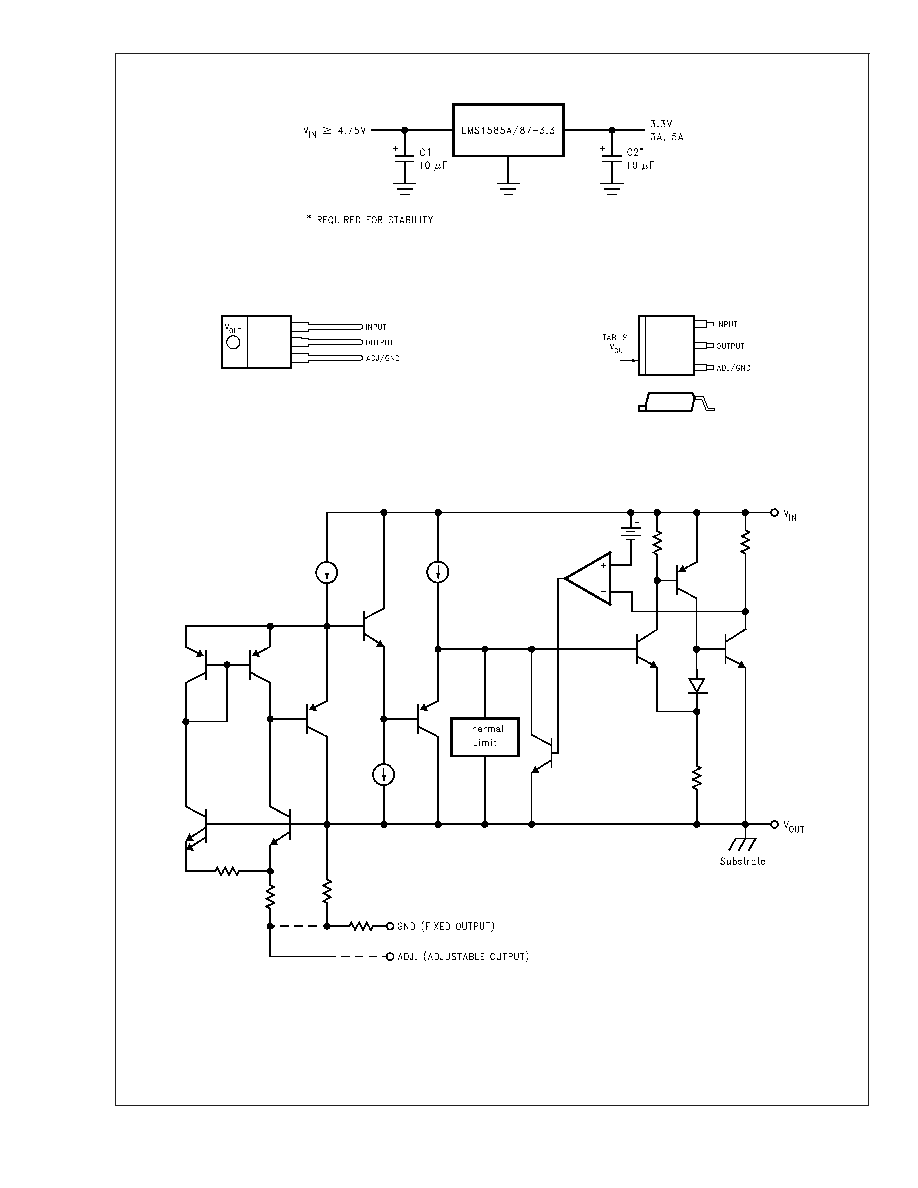
Typical Application
20099801
Connection Diagrams
TO-220
TO-263
20099836
Top View
20099835
Top View
Simplified Schematic
20099814
LMS1585AEP/LMS1587EP
Enhanced
Plastic
www.national.com
2
Absolute Maximum Ratings
(Note 4)
If Military/Aerospace specified devices are required,
please contact the National Semiconductor Sales Office/
Distributors for availability and specifications.
Maximum Input to Output Voltage
(V
IN
to GND)
13V
Power Dissipation (Note 5)
Internally Limited
Junction Temperature (T
J
) (Note 5)
150°C
Storage Temperature Range
-65°C to 150°C
Lead Temperature
260°C, 10 sec
ESD Tolerance (Note 6)
2000V
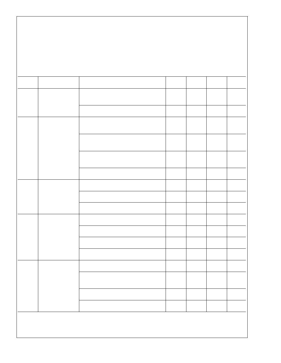
Electrical Characteristics
Typicals and limits appearing in normal type apply for T
J
= 25°C. Limits appearing in Boldface type apply over the entire junc-
tion temperature range for operation, 0°C to 125°C for commercial grade and -40°C to 125°C for Enhanced Plastic.
Symbol
Parameter
Conditions
Min
(Note 8)
Typ
(Note 7)
Max
(Note 8)
Units
V
REF
Reference Voltage
LMS1585A-ADJEP
V
IN
-V
OUT
= 3V, I
OUT
= 10mA
10mA
I
OUT
5A, 1.5V V
IN
-V
OUT
5.75V
1.238
1.225
1.25
1.250
1.262
1.275
V
V
LMS1587-ADJEP
10mA
I
OUT
3A, 1.5V V
IN
-V
OUT
5.75V
1.225
1.250
1.275
V
V
OUT
Output Voltage
LMS1585A-1.5EP
I
OUT
= 0mA, V
IN
= 5V
0
I
OUT
5A, 3V V
IN
7V
1.485
1.470
1.500
1.515
1.530
V
V
LMS1585A-3.3EP
I
OUT
= 0mA, V
IN
= 5V
0
I
OUT
5A, 4.75V V
IN
7V
3.267
3.235
3.300
3.300
3.333
3.365
V
V
LMS1587-1.5EP
V
IN
= 5V, I
OUT
= 0mA, T
J
= 25°C
0
I
OUT
3A, 3V V
IN
7V
1.485
1.470
1.500
1.500
1.515
1.530
V
V
LMS1587-3.3EP
0
I
OUT
3A, 4.75V V
IN
7V
3.235
3.300
3.365
V
V
OUT
Line Regulation
(Note 9)
LMS1585AEP/87-ADJEP
I
OUT
= 10mA, 2.75V
V
IN
7V
0.005
0.2
%
LMS1585AEP/87-3.3EP
I
OUT
= 0mA, 4.75V
V
IN
7V
0.005
0.2
%
LMS1585AEP/87-1.5EP
I
OUT
= 0mA, 3V
V
IN
7V
0.005
0.2
%
V
OUT
Load Regulation
(Note 9)
LMS1585A-ADJEP
V
IN
-V
OUT
= 3V, 10mA
I
OUT
5A
0.05
0.3
0.5
%
LMS1585A-1.5EP/LMS1585A-3.3EP
V
IN
= 5V, 0
I
OUT
5A
0.05
0.05
0.3
0.5
%
LMS1587-ADJEP
V
IN
-V
OUT
= 3V, 10mA
I
OUT
3A
0.05
0.05
0.3
0.5
%
LMS1587-1.5EP/LMS1587-3.3EP
V
IN
= 5V, 0
I
OUT
3A
0.05
0.05
0.3
0.5
%
%
V
IN
-V
OUT
Dropout Voltage
LMS1585A-ADJEP/LMS1587-ADJEP
V
REF
= 1%, I
OUT
= 3A
1.15
1.3
V
LMS1585A-3.3EP/LMS1587-3.3EP/
LMS1585A-1.5EP/LMS1587-1.5EP
V
OUT
= 1%, I
OUT
= 3A
1.15
1.3
V
LMS1585A-ADJEP
V
REF
= 1%, I
OUT
= 5A
1.2
1.4
V
LMS1585A-1.5EP/LMS1585A-3.3EP
V
OUT
= 1%, I
OUT
= 5A
1.2
1.4
V
LMS1585AEP/LMS1587EP
Enhanced
Plastic
www.national.com
3
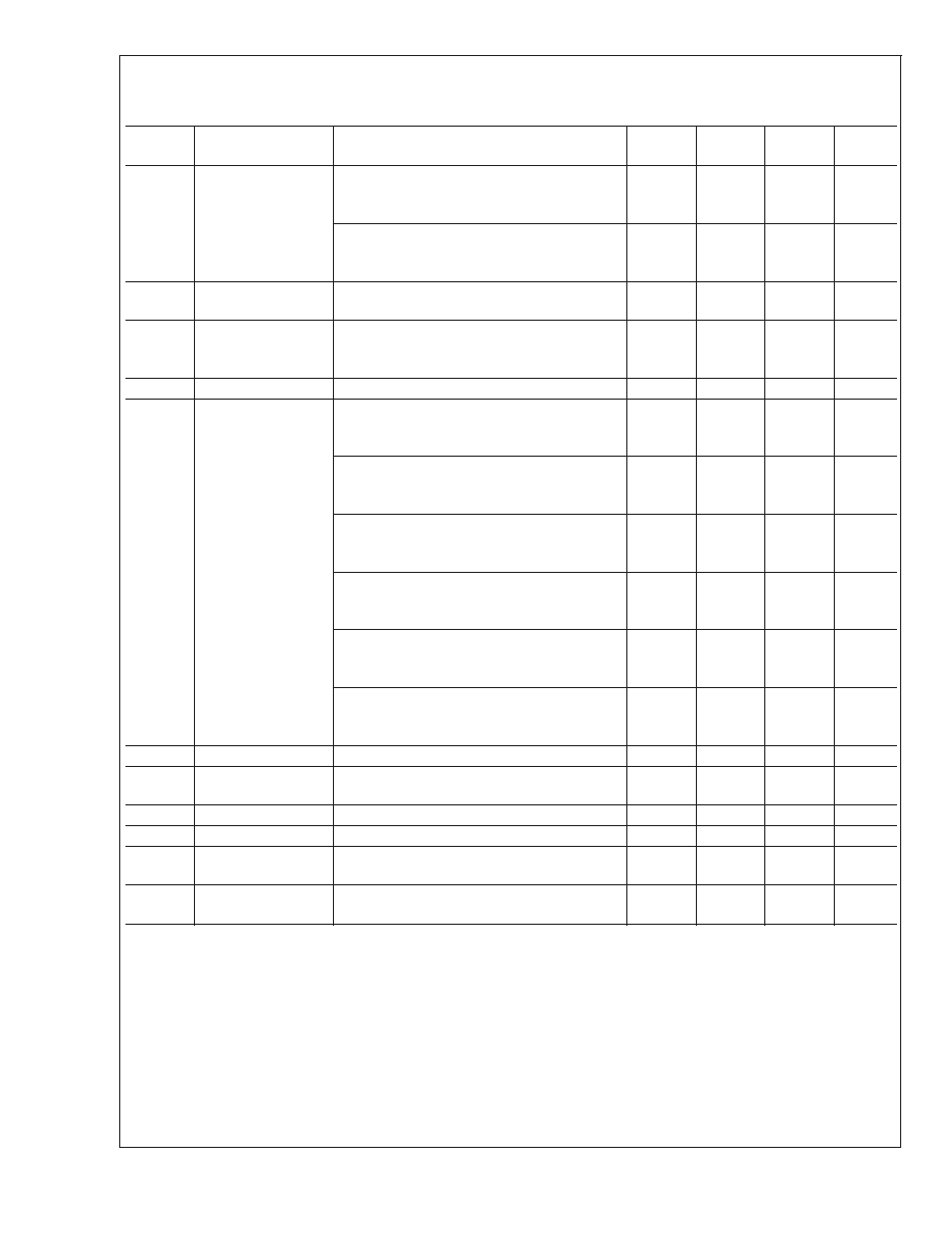
Electrical Characteristics
(Continued)
Typicals and limits appearing in normal type apply for T
J
= 25°C. Limits appearing in Boldface type apply over the entire junc-
tion temperature range for operation, 0°C to 125°C for commercial grade and -40°C to 125°C for Enhanced Plastic.
Symbol
Parameter
Conditions
Min
(Note 8)
Typ
(Note 7)
Max
(Note 8)
Units
I
LIMIT
Current Limit
LMS1585A-ADJEP/LMS1585A-3.3EP/
LMS1585A-1.5EP
V
IN
-V
OUT
= 5.5V
5.0
6.6
A
LMS1587-ADJEP/LMS1587-3.3EP/
LMS1587-1.5EP
V
IN
-V
OUT
= 5.5V
3.1
4.3
A
Minimum Load
Current (Note 10)
LMS1585AEP/87-ADJEP
1.5V
V
IN
-V
OUT
5.75V
2.0
10.0
mA
Quiescent Current
LMS1585A-3.3EP/LMS1587-3.3EP/
LMS1585A-1.5EP/LMS1587-1.5EP
V
IN
= 5V
7.0
13.0
mA
Thermal Regulation
T
A
= 25°C, 30ms Pulse
0.003
%/W
Ripple Rejection
LMS1585A-ADJEP
f
RIPPLE
= 120Hz, V
IN
-V
OUT
= 3V,
I
OUT
= 5A, C
OUT
= 25µF Tantalum
72
dB
LMS1585A-1.5EP
f
RIPPLE
= 120Hz, C
OUT
= 25µF Tantalum,
I
OUT
= 5A, V
IN
= 4.5V
60
72
dB
LMS1585A-3.3EP
f
RIPPLE
= 120Hz, C
OUT
= 25µF Tantalum,
I
OUT
= 5A, V
IN
= 6.3V
72
dB
LMS1587-ADJEP
f
RIPPLE
= 120Hz, V
IN
-V
OUT
= 3V, I
OUT
= 3A
C
OUT
= 25µF Tantalum
72
dB
LMS1587-1.5EP
f
RIPPLE
= 120Hz, C
OUT
= 25µF Tantalum,
I
OUT
= 3A, V
IN
= 4.5V
60
72
dB
LMS1587-3.3EP
f
RIPPLE
= 120Hz, C
OUT
= 25µF Tantalum,
I
OUT
= 3A, V
IN
= 6.3V
72
dB
Adjust Pin Current
55
120
µA
Adjust Pin Current
10mA
I
OUT
I
FULLLOAD
,
1.5V
V
IN
-V
OUT
5.75V (Note 11)
0.2
µA
Temperature Stability
0.5
%
Long Term Stability
T
A
= 125°C, 1000Hrs
0.03
%
RMS Output Noise
(% of V
OUT
)
10Hz
f 10kHz
0.003
%
Thermal Resistance
Junction-to-Case
3-Lead TO-263: Control/Output Section
3-Lead TO-220: Control/Output Section
0.65/2.7
0.65/2.7
°C/W
°C/W
Note 4: Absolute Maximum Ratings indicate limits beyond which damage to the device may occur. Operating Ratings indicate conditions for which the device is
intended to be functional, but specific performance is not guaranteed. For guaranteed specifications and the test conditions, see the Electrical Characteristics.
Note 5: The maximum power dissipation is a function of T
J(max)
,
JA
, and T
A
. The maximum allowable power dissipation at any ambient temperature
is P
D
= (T
J(max)
T
A
)/
JA
. All numbers apply for packages soldered directly into a PC board.
Note 6: For testing purposes, ESD was applied using human body model, 1.5k
in series with 100pF.
Note 7: Typical Values represent the most likely parametric norm.
Note 8: All limits are guaranteed by testing or statistical analysis.
Note 9: Load and line regulation are measured at constant junction temperature, and are guaranteed up to the maximum power dissipation of 30W. Power
dissipation is determined by the input/output differential and the output current. Guaranteed maximum power dissipation will not be available over the full input/output
range.
Note 10: The minimum output current required to maintain regulation.
Note 11: I
FULLLOAD
is 5A for LMS1585AEP and 3A for LMS1587EP.
Note 12: Consult factory for other fixed voltage options.
LMS1585AEP/LMS1587EP
Enhanced
Plastic
www.national.com
4
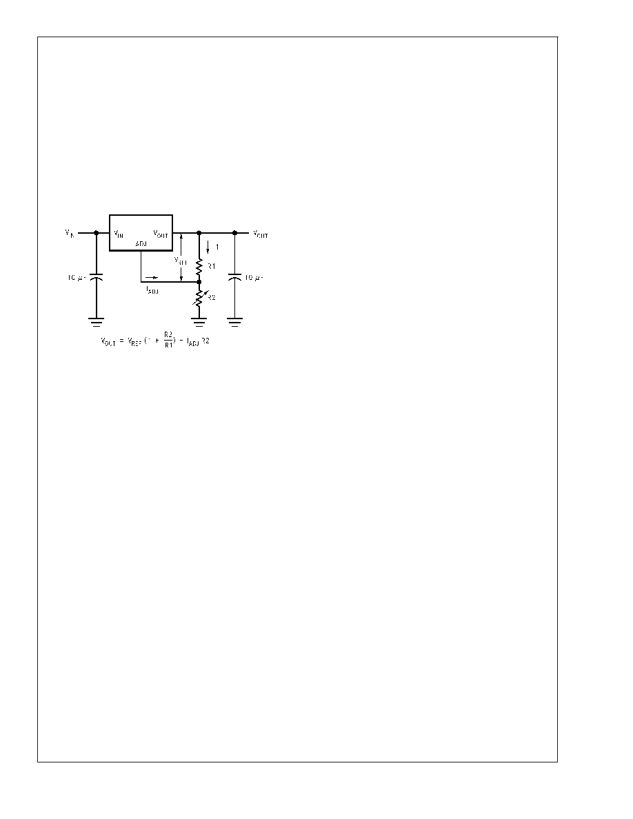
Application Note
Output Voltage
The adjustable version develops at 1.25V reference voltage,
(V
REF
), between the output and the adjust terminal. As
shown in Figure 1, this voltage is applied across resistor R1
to generate a constant current I1. This constant current then
flows through R2. The resulting voltage drop across R2 adds
to the reference voltage to sets the desired output voltage.
The current I
ADJ
from the adjustment terminal introduces an
output error. But since it is small (120µA max), it becomes
negligible when R1 is in the 100
range.
For fixed voltage devices, R1 and R2 are integrated inside
the devices.
20099872
FIGURE 1. Basic Adjustable Regulator
LMS1585AEP/LMS1587EP
Enhanced
Plastic
www.national.com
5
Document Outline