 | –≠–ª–µ–∫—Ç—Ä–æ–Ω–Ω—ã–π –∫–æ–º–ø–æ–Ω–µ–Ω—Ç: LMV712MM | –°–∫–∞—á–∞—Ç—å:  PDF PDF  ZIP ZIP |

LMV712
Low Power, Low Noise, High Output, RRIO Dual
Operational Amplifier with Independent Shutdown
General Description
The LMV712 duals are high performance BiCMOS opera-
tional
amplifiers
intended
for
applications
requiring
Rail-to-Rail inputs combined with speed and low noise. They
offer a bandwidth of 5MHz and a slew rate of 5V/µs and can
handle capacitive loads of up to 200pF without oscillation.
The LMV712 offers two independent shutdown pins. This
feature allows disabling of each device separately and re-
duces the supply current to less than 1µA typical. The output
voltage rapidly ramps up smoothly with no glitch as the
amplifier comes out of the shutdown mode.
The LMV712 with the shutdown feature is offered in space
saving 10-Bump micro SMD and 10 pin Leadless Leadframe
Package (LLP) packages. It is also offered in 10 lead MSOP
package. These packages are designed to meet the de-
mands of small size, low power, and low cost required by
cellular phones and similar battery operated portable elec-
tronics.
Features
(Typical Unless Otherwise Noted)
n
5 MHz GBP
n
Slew rate 5 V/µs
n
Low noise 20nV/
n
Supply current 1.22mA/channel
n
V
OS
<
3mV max.
n
Low supply voltage 2.7V to 5V.
n
Rail-to-Rail inputs and outputs.
n
Unity gain stable.
n
Small package: 10-Pin LLP, 10-Pin MSOP and 10-Bump
micro SMD
n
1.5µA shutdown I
CC
n
2.2µs turn on
Applications
n
Power amplifier control loop
n
Cellular phones
n
Portable equipment
n
Wireless LAN
n
Radio systems
n
Cordless phones
Typical Application Circuit
10137034
P.A. Control Loop
Output Waveform vs. Shutdown
Pulse
10137030
February 2002
LMV712
Low
Power
,
Low
Noise,
High
Output,
RRIO
Dual
Operational
Amplifier
with
Independent
Shutdown
© 2002 National Semiconductor Corporation
DS101370
www.national.com

Absolute Maximum Ratings
(Note 1)
If Military/Aerospace specified devices are required,
please contact the National Semiconductor Sales Office/
Distributors for availability and specifications.
ESD Tolerance (Note 2)
Machine Model
150V
Human Body Model
1.5kV
Differential Input Voltage
±
Supply Voltage
Voltage at Input/Output Pin
(V
+
) +0.4V to (V
-
) -0.4V
Supply Voltage (V
+
- V
-
)
5.5V
Output Short Circuit V
+
(Note 3)
Output Short Circuit V
-
(Note 3)
Current at Input Pin
±
10mA
Current at Output Pin
±
50mA
Storage Temp Range
-65∞C to 150∞C
Mounting Temperature
Infrared or Convection (20
sec)
235∞C
Junction Temperature T
JMAX
(Note 4)
150∞C
Recommended Operating
Conditions
(Note 1)
Supply Voltage
2.7V to 5V
Temperature Range
-40∞C
T
J
85∞C
Thermal Resistance
10-Pin MSOP
235∞C/W
10-Pin LLP
53.4∞C/W
10-Bump micro SMD
196∞C/W
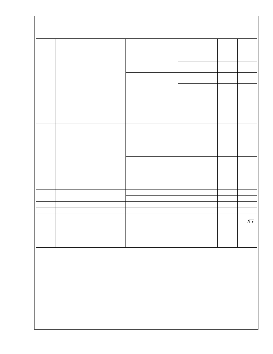
2.7V Electrical Characteristics
Unless otherwise specified, all limits guaranteed for V
+
= 2.7V, V
-
= 0V,
V
CM
= 1.35V and T
A
= 25∞C and R
L
>
1M
. Boldface limits apply at the temperature extremes.
Symbol
Parameter
Condition
Min
(Note 6)
Typ
(Note 5)
Max
(Note 6)
Units
V
OS
Input Offset Voltage
V
CM
= 0.85V and
V
CM
= 1.85V
0.4
3
3.2
mV
I
B
Input Bias Current
5.5
115
130
pA
CMRR
Common Mode Rejection Ratio
0V
V
CM
2.7V
50
45
75
dB
PSRR
Power Supply Rejection Ratio
2.7V
V
+
5V,
V
CM
= 0.85V
70
68
90
dB
2.7V
V
+
5V,
V
CM
= 1.85V
70
68
90
dB
CMVR
Common Mode Voltage Range
For CMRR
50dB
-0.3
-0.2
V
2.9
3
V
I
SC
Output Short Circuit Current
Sourcing
V
O
= 0V
15
12
25
mA
Sinking
V
O
= 2.7V
25
22
50
mA
V
O
Output Swing
R
L
= 10k
to 1.35V
2.62
2.60
2.68
V
0.01
0.12
0.15
V
R
L
= 600
to 1.35V
2.52
2.50
2.55
V
0.05
0.23
0.30
V
V
O
(SD)
Output Voltage in Shutdown
10
200
mV
I
S
Supply Current per Channel
On Mode
1.22
1.7
1.9
mA
Shutdown Mode
0.12
1.5
2.0
uA
LMV712
www.national.com
2

2.7V Electrical Characteristics
Unless otherwise specified, all limits guaranteed for V
+
= 2.7V, V
-
= 0V,
V
CM
= 1.35V and T
A
= 25∞C and R
L
>
1M
. Boldface limits apply at the temperature extremes. (Continued)
Symbol
Parameter
Condition
Min
(Note 6)
Typ
(Note 5)
Max
(Note 6)
Units
A
VOL
Large Signal Voltage Gain
Sourcing
R
L
= 10k
V
O
= 1.35V to 2.3V
80
76
115
dB
Sinking
R
L
= 10k
V
O
= 0.4V to 1.35V
80
76
113
dB
Sourcing
R
L
= 600
V
O
= 1.35V to 2.2V
80
76
97
dB
Sinking
R
L
= 600
V
O
= 0.5V to 1.35V
80
76
100
dB
V
SD
Shutdown Pin Voltage Range
On Mode
2.4 to 2.7
2.0 to 2.7
V
Shutdown Mode
0 to 0.8
0 to 1
V
GBWP
Gain-Bandwidth Product
5
MHz
SR
Slew Rate
(Note 7)
5
V/µs
m
Phase Margin
60
Deg
e
n
Input Referred Voltage Noise
f = 1kHz
20
nV/
T
ON
Turn-On Time from Shutdown
2.2
4
4.6
µs
Turn-On Time from Shutdown
(micro SMD)
6
8
µs
5V Electrical Characteristics
Unless otherwise specified, all limits guaranteed for V
+
=5V, V
-
= 0V, V
CM
= 2.5V and T
A
= 25∞C and R
L
>
1M
. Boldface
limits apply at the temperature extremes.
Symbol
Parameter
Condition
Min
(Note 6)
Typ
(Note 5)
Max
(Note 6)
Units
V
OS
Input Offset Voltage
V
CM
= 0.85V and
V
CM
= 1.85V
0.4
3
3.2
mV
I
B
Input Bias Current
5.5
115
130
pA
CMRR
Common Mode Rejection Ratio
0V
V
CM
5V
50
45
80
dB
PSRR
Power Supply Rejection Ratio
2.7V
V
+
5V,
V
CM
= 0.85V
70
68
90
dB
2.7V
V
+
5V,
V
CM
= 1.85V
70
68
90
dB
CMVR
Common Mode Voltage Range
For CMRR
50dB
-0.3
-0.2
V
5.2
5.3
V
I
SC
Output Short Circuit Current
Sourcing
V
O
= 0V
20
18
35
mA
Sinking
V
O
= 5V
25
21
50
mA
LMV712
www.national.com
3
5V Electrical Characteristics
(Continued)
Unless otherwise specified, all limits guaranteed for V
+
=5V, V
-
= 0V, V
CM
= 2.5V and T
A
= 25∞C and R
L
>
1M
. Boldface
limits apply at the temperature extremes.
Symbol
Parameter
Condition
Min
(Note 6)
Typ
(Note 5)
Max
(Note 6)
Units
V
O
Output Swing
R
L
= 10k
to 2.5V
4.92
4.90
4.98
V
0.01
0.12
0.15
V
R
L
= 600
to 2.5V
4.82
4.80
4.85
V
0.05
0.23
0.30
V
V
O
(SD)
Output Voltage in Shutdown
10
200
mV
I
S
Supply Current per Channel
On Mode
1.17
1.7
1.9
mA
Shutdown Mode
0.12
1.5
2.0
uA
A
VOL
Large Signal Voltage Gain
Sourcing
R
L
= 10k
V
O
= 2.5V to 4.6V
80
76
130
dB
Sinking
R
L
= 10k
V
O
= 0.4V to 2.5V
80
76
130
dB
Sourcing
R
L
= 600
V
O
= 2.5V to 4.6V
80
76
110
dB
Sinking
R
L
= 600
V
O
= 0.4V to 2.5V
80
76
107
dB
V
SD
Shutdown Pin Voltage Range
On Mode
4.5 to 5
3.5 to 5
V
Shutdown Mode
0 to 0.8
0 to 1.5
V
GBWP
Gain-Bandwidth Product
5
MHz
SR
Slew Rate
(Note 7)
5
V/µs
m
Phase Margin
60
Deg
e
n
Input Referred Voltage Noise
f = 1kHz
20
nV/
T
ON
Turn-On Time for Shutdown
1.6
4
4.6
µs
Turn-On Time for Shutdown
(micro SMD)
6
8
µs
Note 1: Absolute Maximum Ratings indicate limits beyond which damage to the device may occur. Operating Ratings indicate conditions for which the device is
intended to be functional, but specific performance is not guaranteed. For guaranteed specifications and the test conditions, see the Electrical Characteristics.
Note 2: Human body model: 1.5k
in series with 100pF. Machine model, 0
in series with 100pF.
Note 3: Shorting circuit output to either V
+
or V
-
will adversely affect reliability.
Note 4: The maximum power dissipation is a function of T
J(MAX)
,
JA
and T
A
. The maximum allowable power dissipation at any ambient temperature is P
D
=
(T
J(MAX)
-T
A
)/
JA
. All numbers apply for packages soldered directly into a PC board.
Note 5: Typical values represent the most likely parametric norm.
Note 6: All limits are guaranteed by testing or statistical analysis.
Note 7: Number specified is the slower of the positive and negative slew rates.
LMV712
www.national.com
4

Typical Performance Characteristics
Unless otherwise specified, V
S
= +5V, single suppy, T
A
=
25∞C.
Supply Current Per Channel vs. Supply Voltage
Supply Current vs. Supply Voltage (Shutdown)
10137001
10137002
V
OS
vs. V
CM
I
B
vs. V
CM
Over Temp
10137003
10137005
Output Positive Swing vs. Supply Voltage, R
L
= 600
Output Negative Swing vs. Supply Voltage, R
L
= 600
10137006
10137007
LMV712
www.national.com
5