
LMX2330L/LMX2331L/LMX2332L
PLLatinum
TM
Low Power Dual Frequency Synthesizer for
RF Personal Communications
LMX2330L
2.5 GHz/510 MHz
LMX2331L
2.0 GHz/510 MHz
LMX2332L
1.2 GHz/510 MHz
General Description
The LMX233XL family of monolithic, integrated dual fre-
quency synthesizers, including prescalers, is to be used as a
local oscillator for RF and first IF of a dual conversion
transceiver. It is fabricated using National's 0.5µ ABiC V
silicon BiCMOS process.
The LMX233XL contains dual modulus prescalers. A 64/65
or a 128/129 prescaler (32/33 or 64/65 in the 2.5 GHz
LMX2330L) can be selected for the RF synthesizer and a 8/9
or a 16/17 prescaler can be selected for the IF synthesizer.
LMX233XL, which employs a digital phase locked loop tech-
nique, combined with a high quality reference oscillator,
provides the tuning voltages for voltage controlled oscillators
to generate very stable, low noise signals for RF and IF local
oscillators. Serial data is transferred into the LMX233XL via
a three wire interface (Data, Enable, Clock). Supply voltage
can range from 2.7V to 5.5V. The LMX233XL family features
very low current consumption;
LMX2330L -- 5.0 mA at 3V, LMX2331L -- 4.0 mA at 3V,
LMX2332L -- 3.0 mA at 3V.
The LMX233XL are available in a TSSOP 20-pin, CSP
24-pin surface mount plastic package, and thin CSP 20-pin
surface mount plastic package.
Features
n
Ultra low current consumption
n
2.7V to 5.5V operation
n
Selectable synchronous or asynchronous powerdown
mode:
I
CC
= 1 µA typical at 3V
n
Dual modulus prescaler:
LMX2330L
(RF) 32/33 or 64/65
LMX2331L/32L
(RF) 64/65 or 128/129
LMX2330L/31L/32L
(IF) 8/9 or 16/17
n
Selectable charge pump TRI-STATE
Æ
mode
n
Selectable charge pump current levels
n
Selectable Fastlock
TM
mode
n
Upgrade and compatible to LMX233XA family
Applications
n
Portable Wireless Communications
(PCS/PCN, cordless)
n
Cordless and cellular telephone systems
n
Wireless Local Area Networks (WLANs)
n
Cable TV tuners (CATV)
n
Other wireless communication systems
Functional Block Diagram
01280601
October 2001
LMX2330L/LMX2331L/LMX2332L
PLLatinum
Low
Power
Dual
Frequency
Synthesizer
for
RF
Personal
Communications
© 2001 National Semiconductor Corporation
DS012806
www.national.com

Connection Diagrams
Chip Scale Package (SLB)
(Top View)
Thin Shrink Small Outline Package (TM)
(Top View)
01280639
Order Number LMX2330LSBX, LMX2331LSLBX or
LMX2332LSLBX
NS Package Number SLB24A
01280602
Order Number LMX2330LTM, LMX2331LTM or
LMX2332LTM
Order Number LMX2330LTMX, LMX2331LTMX, or
LMX2332LTMX
NS Package Number MTC20
20-Pin Thin Chipscale Package (SLD)
(Top View)
01280640
Order Number LMX2330LSLDX, LMX2331LSLDX, or
LMX2332LSLDX
NS Package Number SLD20A
LMX2330L/LMX2331L/LMX2332L
www.national.com
2

Pin Descriptions
Pin No.
LMX233XLSLD
20-pin Thin
CSP Package
Pin No.
LMX233XLSLB
24-pin CSP
Package
Pin No.
LMX233XLTM
20-pin TSSOP
Package
Pin
Name
I/O
Description
20
24
1
V
CC
1
--
Power supply voltage input for RF analog and RF digital circuits.
Input may range from 2.7V to 5.5V. V
CC
1 must equal V
CC
2.
Bypass capacitors should be placed as close as possible to this
pin and be connected directly to the ground plane.
1
2
2
V
P
1
--
Power Supply for RF charge pump. Must be
V
CC
.
2
3
3
D
o
RF
O
Internal charge pump output. For connection to a loop filter for
driving the input of an external VCO.
3
4
4
GND
--
Ground for RF digital circuitry.
4
5
5
f
IN
RF
I
RF prescaler input. Small signal input from the VCO.
5
6
6
f
IN
RF
I
RF prescaler complementary input. A bypass capacitor should
be placed as close as possible to this pin and be connected
directly to the ground plane. Capacitor is optional with some loss
of sensitivity.
6
7
7
GND
--
Ground for RF analog circuitry.
7
8
8
OSC
in
I
Oscillator input. The input has a V
CC
/2 input threshold and can
be driven from an external CMOS or TTL logic gate.
8
10
9
GND
--
Ground for IF digital, MICROWIRE
TM
, F
o
LD, and oscillator
circuits.
9
11
10
F
o
LD
O
Multiplexed output of the RF/IF programmable or reference
dividers, RF/IF lock detect signals and Fastlock mode. CMOS
output
(see Programmable Modes).
10
12
11
Clock
I
High impedance CMOS Clock input. Data for the various
counters is clocked in on the rising edge, into the 22-bit shift
register.
11
14
12
Data
I
Binary serial data input. Data entered MSB first. The last two bits
are the control bits. High impedance CMOS input.
12
15
13
LE
I
Load enable high impedance CMOS input. When LE goes HIGH,
data stored in the shift registers is loaded into one of the 4
appropriate latches (control bit dependent).
13
16
14
GND
--
Ground for IF analog circuitry.
14
17
15
f
IN
IF
I
IF prescaler complementary input. A bypass capacitor should be
placed as close as possible to this pin and be connected directly
to the ground plane. Capacitor is optional with some loss of
sensitivity.
15
18
16
f
IN
RF
I
IF prescaler input. Small signal input from the VCO.
16
19
17
GND
--
Ground for IF digital, MICROWIRE, F
o
LD, and oscillator circuits.
17
20
18
D
o
IF
O
IF charge pump output. For connection to a loop filter for driving
the input of an external VCO.
18
22
19
V
P
2
--
Power Supply for IF charge pump. Must be
V
CC
.
19
23
20
V
CC
2
--
Power supply voltage input for IF analog, IF digital,
MICROWIRE, F
o
LD, and oscillator circuits. Input may range from
2.7V to 5.5V. V
CC
2 must equal V
CC
1. Bypass capacitors should
be placed as close as possible to this pin and be connected
directly to the ground plane.
X
1, 9, 13, 21
X
NC
--
No connect.
LMX2330L/LMX2331L/LMX2332L
www.national.com
3
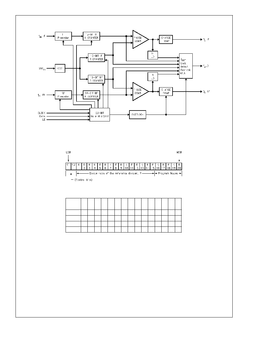
Block Diagram
01280603
Note: The RF prescaler for the LMX2331L/32L is either 64/65 or 128/129, while the prescaler for the LMX2330L is 32/33 or 64/65.
Note: V
CC
1 supplies power to the RF prescaler, N-counter, R-counter and phase detector. V
CC
2 supplies power to the IF prescaler, N-counter, phase detector,
R-counter along with the OSC
in
buffer, MICROWIRE, and F
o
LD. V
CC
1 and V
CC
2 are clamped to each other by diodes and must be run at the same voltage level.
Note: V
P
1 and V
P
2 can be run separately as long as V
P
V
CC
.
LMX2330L/LMX2331L/LMX2332L
www.national.com
4

Absolute Maximum Ratings
(Notes 1,
2)
If Military/Aerospace specified devices are required,
please contact the National Semiconductor Sales Office/
Distributors for availability and specifications.
Power Supply Voltage
V
CC
-0.3V to +6.5V
V
P
-0.3V to +6.5V
Voltage on Any Pin
with GND = 0V (V
I
)
-0.3V to V
CC
+0.3V
Storage Temperature Range (T
S
)
-65∞C to +150∞C
Lead Temperature (solder 4 sec.)
(T
L
)
+260∞C
Recommended Operating
Conditions
Power Supply Voltage
V
CC
2.7V to 5.5V
V
P
V
CC
to +5.5V
Operating Temperature (T
A
)
-40∞C to +85∞C
Note 1: Absolute Maximum Ratings indicate limits beyond which damage to
the device may occur. Recommended Operating Conditions indicate condi-
tions for which the device is intended to be functional, but do not guarantee
specific performance limits. For guaranteed specifications and test condi-
tions, see the Electrical Characteristics. The guaranteed specifications apply
only for the test conditions listed.
Note 2: This device is a high performance RF integrated circuit with an ESD
rating
<
2 keV and is ESD sensitive. Handling and assembly of this device
should only be done at ESD protected work stations.
Electrical Characteristics
V
CC
= 3.0V, V
P
= 3.0V; -40∞C
<
T
A
<
85∞C, except as specified
Symbol
Parameter
Conditions
Value
Units
Min
Typ
Max
I
CC
Power
LMX2330L RF + IF
V
CC
= 2.7V to 5.5V
5.0
6.6
Supply
LMX2330L RF Only
4.0
5.2
Current
LMX2331L RF + IF
4.0
5.4
LMX2331L RF Only
3.0
4.0
mA
LMX2332L IF + RF
3.0
4.1
LMX2332L RF Only
2.0
2.7
LMX233xL IF Only
1.0
1.4
I
CC-PWDN
Powerdown Current
(Note 3)
1
10
µA
f
IN
RF
Operating
LMX2330L
0.5
2.5
Frequency
LMX2331L
0.2
2.0
GHz
LMX2332L
0.1
1.2
f
IN
IF
Operating
LMX233xL
45
510
MHz
Frequency
f
OSC
Oscillator Frequency
5
40
MHz
f
Maximum Phase Detector
10
MHz
Frequency
Pf
IN
RF
RF Input Sensitivity
V
CC
= 3.0V
-15
0
dBm
V
CC
= 5.0V
-10
0
dBm
Pf
IN
IF
IF Input Sensitivity
V
CC
= 2.7V to 5.5V
-10
0
dBm
V
OSC
Oscillator Sensitivity
OSC
in
0.5
V
PP
V
IH
High-Level Input Voltage
(Note 4)
0.8 V
CC
V
V
IL
Low-Level Input Voltage
(Note 4)
0.2 V
CC
V
I
IH
High-Level Input Current
V
IH
= V
CC
= 5.5V (Note
4)
-1.0
1.0
µA
I
IL
Low-Level Input Current
V
IL
= 0V, V
CC
= 5.5V
(Note 4)
-1.0
1.0
µA
I
IH
Oscillator Input Current
V
IH
= V
CC
= 5.5V
100
µA
I
IL
Oscillator Input Current
V
IL
= 0V, V
CC
= 5.5V
-100
µA
V
OH
High-Level Output Voltage (for
F
o
LD, pin number 10)
I
OH
= -500 µA
V
CC
- 0.4
V
V
OL
Low-Level Output Voltage (for
F
o
LD, pin number 10)
I
OL
= 500 µA
0.4
V
t
CS
Data to Clock Set Up Time
See Data Input Timing
50
ns
t
CH
Data to Clock Hold Time
See Data Input Timing
10
ns
LMX2330L/LMX2331L/LMX2332L
www.national.com
5
Electrical Characteristics
(Continued)
V
CC
= 3.0V, V
P
= 3.0V; -40∞C
<
T
A
<
85∞C, except as specified
Symbol
Parameter
Conditions
Value
Units
Min
Typ
Max
t
CWH
Clock Pulse Width High
See Data Input Timing
50
ns
t
CWL
Clock Pulse Width Low
See Data Input Timing
50
ns
t
ES
Clock to Load Enable Set Up Time
See Data Input Timing
50
ns
t
EW
Load Enable Pulse Width
See Data Input Timing
50
ns
Note 3: Clock, Data and LE = GND or V
cc
.
Note 4: Clock, Data and LE does not include f
IN
RF, f
IN
IF and OSC
IN
.
Charge Pump Characteristics
V
CC
= 3.0V, V
P
= 3.0V; -40∞C
<
T
A
85∞C, except as specified
Symbol
Parameter
Conditions
Value
Units
Min
Typ
Max
I
Do
-SOURCE
Charge Pump Output
V
Do
= V
P
/2, I
CPo
= HIGH (Note 5)
-4.0
mA
I
Do
-SINK
Current
V
Do
= V
P
/2, I
CPo
= HIGH (Note 5)
4.0
mA
I
Do
-SOURCE
V
Do
= V
P
/2, I
CPo
= LOW (Note 5)
-1
mA
I
Do
-SINK
V
Do
= V
P
/2, I
CPo
= LOW (Note 5)
1
mA
I
Do
-TRI
Charge Pump
0.5V
V
Do
V
P
- 0.5V
-2.5
2.5
nA
TRI-STATE Current
-40∞C
<
T
A
<
85∞C
I
Do
-SINK vs
CP Sink vs
V
Do
= V
P
/2
3
10
%
I
Do-
SOURCE
Source Mismatch (Note 7)
T
A
= 25∞C
I
Do
vs V
Do
CP Current vs Voltage
0.5
V
Do
V
P
- 0.5V
10
15
%
(Note 6)
T
A
= 25∞C
I
Do
vs T
A
CP Current vs
V
Do
= V
P
/2
10
%
Temperature (Note 8)
-40∞C
T
A
85∞C
Note 5: See PROGRAMMABLE MODES for I
CPo
description.
LMX2330L/LMX2331L/LMX2332L
www.national.com
6
Charge Pump Current Specification Definitions
01280637
I1 = CP sink current at V
Do
= V
P
-
V
I2 = CP sink current at V
Do
= V
P
/2
I3 = CP sink current at V
Do
=
V
I4 = CP source current at V
Do
= V
P
-
V
I5 = CP source current at V
Do
= V
P
/2
I6 = CP source current at V
Do
=
V
V = Voltage offset from positive and negative rails. Dependent on VCO tuning range relative to V
CC
and ground. Typical values are between 0.5V and 1.0V.
Note 6: I
Do
vs V
Do
=
Charge Pump Output Current magnitude variation vs Voltage =
[
1
/
2
*
{|I1| - |I3|}]/[
1
/
2
*
{|I1| + |I3|}]
*
100%
and
[
1
/
2
*
{|I4| - |I6|}]/[
1
/
2
*
{|I4| + |I6|}]
*
100%
Note 7: I
Do-sink
vs I
Do-source
=
Charge Pump Output Current Sink vs Source Mismatch =
[|I2| - |I5|]/[
1
/
2
*
{|I2| + |I5|}]
*
100%
Note 8: I
Do
vs T
A
=
Charge Pump Output Current magnitude variation vs Temperature =
[|I2
@
temp| - |I2
@
25∞C|]/|I2
@
25∞C|
*
100%
and
[|I5
@
temp| - |I5
@
25∞C|]/|I5
@
25∞C|
*
100%
LMX2330L/LMX2331L/LMX2332L
www.national.com
7
RF Sensitivity Test Block Diagram
01280638
Note 1: N = 10,000
R = 50
P = 64
Note 2: Sensitivity limit is reached when the error of the divided RF output, F
o
LD, is
1 Hz.
Typical Performance
Characteristics
I
CC
vs V
CC
LMX2330L
I
CC
vs V
CC
LMX2331L
01280619
01280620
I
CC
vs V
CC
LMX2332L
I
Do
TRI-STATE
vs D
o
Voltage
01280621
01280622
LMX2330L/LMX2331L/LMX2332L
www.national.com
8
Typical Performance Characteristics
(Continued)
Charge Pump Current vs D
o
Voltage
I
CP
= HIGH
Charge Pump Current vs D
o
Voltage
I
CP
= LOW
01280623
01280624
Charge Pump Current Variation
(See (Note 6) under Charge Pump Current
Specification Definitions)
Sink vs Source Mismatch
(See (Note 7) under Charge Pump Current
Specification Definitions)
01280625
01280626
LMX2330L/LMX2331L/LMX2332L
www.national.com
9
Typical Performance Characteristics
(Continued)
RF Input Impedance
V
CC
= 2.7V to 5.5V, f
IN
= 50 MHz to 3 GHz
IF Input Impedance
V
CC
= 2.7V to 5.5V, f
IN
= 50 MHz to 1000 MHz
01280627
01280628
LMX2330L/LMX2331L/LMX2332L
www.national.com
10
Typical Performance Characteristics
(Continued)
LMX233xSLD RF Input Impedance
V
CC
= 2.7V to 5.5V, f
IN
= 500 MHz to 3 GHz, f
IN
RF CAP =
100 pF
LMX233xSLD IF Input Impedance
V
CC
= 2.7V to 5.5V, f
IN
IF = 100 MHz to 400 MHz, f
IN
IF
CAP = 100 pF
01280641
Marker 1 = 500 MHz,
Real = 202.98,
Imaginary = -200.09
Marker 2 = 1.8 GHz,
Real = 32.36,
Imaginary = -91.42
Marker 3 = 2.5GHz,
Real = 25.51,
Imaginary = -46.41
Marker 4 = 3.0 GHz,
Real = 30.46,
Imaginary = -9.50
01280642
Marker 1 = 100 MHz,
Real = 374.33,
Imaginary = -301.45
Marker 2 = 200 MHz,
Real = 257.14,
Imaginary = -245.79
Marker 3 = 300 MHz,
Real = 194.08,
Imagniary = -224.24
Marker 4 = 400 MHz,
Real = 89.03,
Imaginary = -131.21
LMX2330L RF Sensitivity vs Frequency
LMX2331L RF Sensitivity vs Frequency
01280629
01280630
LMX2330L/LMX2331L/LMX2332L
www.national.com
11
Typical Performance Characteristics
(Continued)
LMX2332L RF Sensitivity vs Frequency
IF Input Sensitivity vs Frequency
01280631
01280632
Oscillator Input Sensitivity vs Frequency
01280633
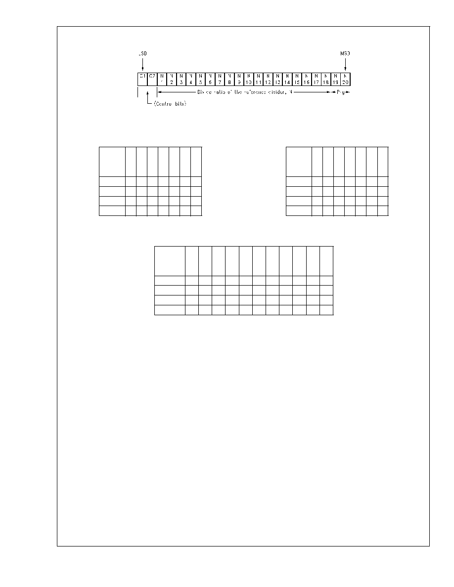
Functional Description
The simplified block diagram below shows the 22-bit data register, two 15-bit R Counters and the 15- and 18-bit N Counters
(intermediate latches are not shown). The data stream is clocked (on the rising edge of Clock) into the DATA register, MSB first.
The data stored in the shift register is loaded into one of 4 appropriate latches on the rising edge of LE. The last two bits are the
Control Bits. The DATA is transferred into the counters as follows:
Control Bits
DATA Location
C1
C2
0
0
IF R Counter
0
1
RF R Counter
1
0
IF N Counter
1
1
RF N Counter
LMX2330L/LMX2331L/LMX2332L
www.national.com
12
Functional Description
(Continued)
01280606
PROGRAMMABLE REFERENCE DIVIDERS (IF AND RF R COUNTERS)
If the Control Bits are 00 or 01 (00 for IF and 01 for RF) data is transferred from the 22-bit shift register into a latch which sets
the 15-bit R Counter. Serial data format is shown below.
01280607
15-BIT PROGRAMMABLE REFERENCE DIVIDER RATIO (R COUNTER)
Divide
R
R
R
R
R
R
R
R
R
R
R
R
R
R
R
Ratio
15 14 13 12 11 10
9
8
7
6
5
4
3
2
1
3
0
0
0
0
0
0
0
0
0
0
0
0
0
1
1
4
0
0
0
0
0
0
0
0
0
0
0
0
1
0
0
∑
∑
∑
∑
∑
∑
∑
∑
∑
∑
∑
∑
∑
∑
∑
∑
32767
1
1
1
1
1
1
1
1
1
1
1
1
1
1
1
Notes:
Divide ratios less than 3 are prohibited.
Divide ratio: 3 to 32767
R1 to R15: These bits select the divide ratio of the programmable reference divider.
Data is shifted in MSB first.
PROGRAMMABLE DIVIDER (N COUNTER)
The N counter consists of the 7-bit swallow counter (A counter) and the 11-bit programmable counter (B counter). If the Control
Bits are 10 or 11 (10 for IF counter and 11 for RF counter) data is transferred from the 22-bit shift register into a 4-bit or 7-bit latch
(which sets the Swallow (A) Counter) and an 11-bit latch (which sets the 11-bit programmable (B) Counter), MSB first. Serial data
format is shown below. For the IF N counter bits 5, 6, and 7 are don't care bits. The RF N counter does not have don't care
bits.
LMX2330L/LMX2331L/LMX2332L
www.national.com
13
Functional Description
(Continued)
01280608
7-BIT SWALLOW COUNTER DIVIDE RATIO (A COUNTER)
RF
Divide
N
7
N
6
N
5
N
4
N
3
N
2
N
1
Ratio
A
0
0
0
0
0
0
0
0
1
0
0
0
0
0
0
1
∑
∑
∑
∑
∑
∑
∑
∑
127
1
1
1
1
1
1
1
Notes: Divide ratio: 0 to 127
B
A
IF
Divide
N
7
N
6
N
5
N
4
N
3
N
2
N
1
Ratio
A
0
X
X
X
0
0
0
0
1
X
X
X
0
0
0
1
∑
∑
∑
∑
∑
∑
∑
∑
15
X
X
X
1
1
1
1
X = DON'T CARE condition
11-BIT PROGRAMMABLE COUNTER DIVIDE RATIO (B COUNTER)
Divide
N
18
N
17
N
16
N
15
N
14
N
13
N
12
N
11
N
10
N
9
N
8
Ratio
B
3
0
0
0
0
0
0
0
0
0
1
1
4
0
0
0
0
0
0
0
0
1
0
0
∑
∑
∑
∑
∑
∑
∑
∑
∑
∑
∑
∑
2047
1
1
1
1
1
1
1
1
1
1
1
Note: Divide ratio: 3 to 2047 (Divide ratios less than 3 are prohibited)
B
A
PULSE SWALLOW FUNCTION
f
VCO
= [(P x B) + A] x f
OSC
/R
f
VCO
: Output frequency of external voltage controlled oscillator (VCO)
B:
Preset divide ratio of binary 11-bit programmable counter (3 to 2047)
A:
Preset divide ratio of binary 7-bit swallow counter
(0
A
127 {RF}, 0
A
15 {IF}, A
B)
f
OSC
: Output frequency of the external reference frequency oscillator
R:
Preset divide ratio of binary 15-bit programmable reference counter (3 to 32767)
P:
Preset modulus of dual moduIus prescaler (for IF; P = 8 or 16;
for RF; LMX2330L: P = 32 or 64
LMX2331L/32L: P = 64 or 128)
LMX2330L/LMX2331L/LMX2332L
www.national.com
14

Functional Description
(Continued)
PROGRAMMABLE MODES
Several modes of operation can be programmed with bits R16≠R20 including the phase detector polarity, charge pump
TRI-STATE and the output of the F
o
LD pin. The prescaler and powerdown modes are selected with bits N19 and N20. The
programmable modes are shown in
Table 1. Truth table for the programmable modes and F
o
LD output are shown in
Table 2 and
Table 3.
TABLE 1. Programmable Modes
C1
C2
R16
R17
R18
R19
R20
0
0
IF Phase
IF I
CPo
IF D
o
IF LD
IF F
o
Detector Polarity
TRI-STATE
0
1
RF Phase
RF I
CPo
RF D
o
RF LD
RF F
o
Detector Polarity
TRI-STATE
C1
C2
N19
N20
1
0
IF Prescaler
Pwdn IF
1
1
RF Prescaler
Pwdn RF
TABLE 2. Mode Select Truth Table
Phase Detector Polarity
D
o
TRI-STATE
I
CPo
IF
2330L RF
2331L/32L RF
Pwdn
(Note 11)
(Note 9)
(Note 10)
Prescaler
Prescaler
Prescaler
(Note 9)
0
Negative
Normal Operation
LOW
8/9
32/33
64/65
Pwrd Up
1
Positive
TRI-STATE
HIGH
16/17
64/65
128/129
Pwrd Dn
Note 9: Refer to POWERDOWN OPERATION in Functional Description.
Note 10: The I
CPo
LOW current state = 1/4 x I
CPo
HIGH current.
Note 11: PHASE DETECTOR POLARITY
Depending upon VCO characteristics, R16 bit should be set accordingly: (see figure right)
When VCO characteristics are positive like (1), R16 should be set HIGH;
When VCO characteristics are negative like (2), R16 should be set LOW.
VCO Characteristics
01280609
LMX2330L/LMX2331L/LMX2332L
www.national.com
15
Functional Description
(Continued)
TABLE 3. The F
o
LD (Pin 10) Output Truth Table
RF R[19]
IF R[19]
RF R[20]
IF R[20]
F
o
Output State
(RF LD)
(IF LD)
(RF F
o
)
(IF F
o
)
0
0
0
0
Disabled (Note 12)
0
1
0
0
IF Lock Detect (Note 13)
1
0
0
0
RF Lock Detect (Note 13)
1
1
0
0
RF/IF Lock Detect (Note 13)
X
0
0
1
IF Reference Divider Output
X
0
1
0
RF Reference Divider Output
X
1
0
1
IF Programmable Divider Output
X
1
1
0
RF Programmable Divider Output
0
0
1
1
Fastlock (Note 14)
0
1
1
1
IF Counter Reset (Note 15)
1
0
1
1
RF Counter Reset (Note 15)
1
1
1
1
IF and RF Counter Reset (Note 15)
X = don't care condition
Note 12: When the F
o
LD output is disabled, it is actively pulled to a low logic state.
Note 13: Lock detect output provided to indicate when the VCO frequency is in "lock." When the loop is locked and a lock detect mode is selected, the pins output
is HIGH, with narrow pulses LOW. In the RF/IF lock detect mode a locked condition is indicated when RF and IF are both locked.
Note 14: The Fastlock mode utilizes the F
o
LD output pin to switch a second loop filter damping resistor to ground during fastlock operation. Activation of Fastlock
occurs whenever the RF loop's lcpo magnitude bit #17 is selected HIGH (while the #19 and #20 mode bits are set for Fastlock).
Note 15: The IF Counter Reset mode resets IF PLL's R and N counters and brings IF charge pump output to a TRI-STATE condition. The RF Counter Reset mode
resets RF PLL's R and N counters and brings RF charge pump output to a TRI-STATE condition. The IF and RF Counter Reset mode resets all counters and brings
both charge pump outputs to a TRI-STATE condition. Upon removal of the Reset bits then N counter resumes counting in "close" alignment with the R counter. (The
maximum error is one prescaler cycle.)
POWERDOWN OPERATION
Synchronous and asynchronous powerdown modes are both available by MICROWIRE selection. Synchronously powerdown
occurs if the respective loop's R18 bit (Do TRI-STATE) is LOW when its N20 bit (Pwdn) becomes HI. Asynchronous powerdown
occurs if the loop's R18 bit is HI when its N20 bit becomes HI.
In the synchronous powerdown mode, the powerdown function is gated by the charge pump to prevent unwanted frequency
jumps. Once the powerdown program bit N20 is loaded, the part will go into powerdown mode when the charge pump reaches
a TRI-STATE condition.
In the asynchronous powerdown mode, the device powers down immediately after the LE pin latches in a HI condition on the
powerdown bit N20.
Activation of either the IF or RF PLL powerdown conditions in either synchronous or asynchronous modes forces the respective
loop's R and N dividers to their load state condition and debiasing of its respective f
IN
input to a high impedance state. The
oscillator circuitry function does not become disabled until both IF and RF powerdown bits are activated. The MICROWIRE
control register remains active and capable of loading and latching data during all of the powerdown modes.
The device returns to an actively powered up condition in either synchronous or asynchronous modes immediately upon LE
latching LOW data into bit N20.
Powerdown Mode Select Table
R18
N20
Powerdown Status
0
0
PLL Active
1
0
PLL Active
(Charge Pump Output TRI-STATE)
0
1
Synchronous Powerdown Initiated
1
1
Asynchronous Powerdown Initiated
LMX2330L/LMX2331L/LMX2332L
www.national.com
16

Functional Description
(Continued)
SERIAL DATA INPUT TIMING
01280610
Note 1: Parenthesis data indicates programmable reference divider data.
Data shifted into register on clock rising edge.
Data is shifted in MSB first.
Note 2: t
cs
= Data to Clock Set-Up Time
t
CH
= Data to Clock Hold Time
t
CWH
= Clock Pulse Width High
t
CWL
= Clock Pulse Width Low
t
ES
= Clock to Load Enable Set-Up Time
t
EW
= Load Enable Pulse Width
Test Conditions: The Serial Data Input Timing is tested using a symmetrical waveform around V
CC
/2. The test waveform has an edge rate of 0.6 V/ns with
amplitudes of 2.2V
@
V
CC
= 2.7V and 2.6V
@
V
CC
= 5.5V.
PHASE COMPARATOR AND INTERNAL CHARGE PUMP CHARACTERISTICS
01280611
Notes: Phase difference detection range: -2
to +2
The minimum width pump up and pump down current pulses occur at the D
o
pin when the loop is locked.
R16 = HIGH
LMX2330L/LMX2331L/LMX2332L
www.national.com
17

Typical Application Example
01280612
Operational Notes:
*
VCO is assumed AC coupled.
**
R
IN
increases impedance so that VCO output power is provided to the load rather than the PLL. Typical values are 10
to 200
depending on the VCO
power level. f
IN
RF impedance ranges from 40
to 100
. f
IN
IF impedances are higher.
***
Adding RC filters to the V
CC
lines is recommended to reduce loop-to-loop noise coupling.
01280613
Application Hints:
Proper use of grounds and bypass capacitors is essential to achieve a high level of performance. Crosstalk between pins can be reduced by careful
board layout.
This is an electrostatic sensitive device. It should be handled only at static free work stations.
LMX2330L/LMX2331L/LMX2332L
www.national.com
18
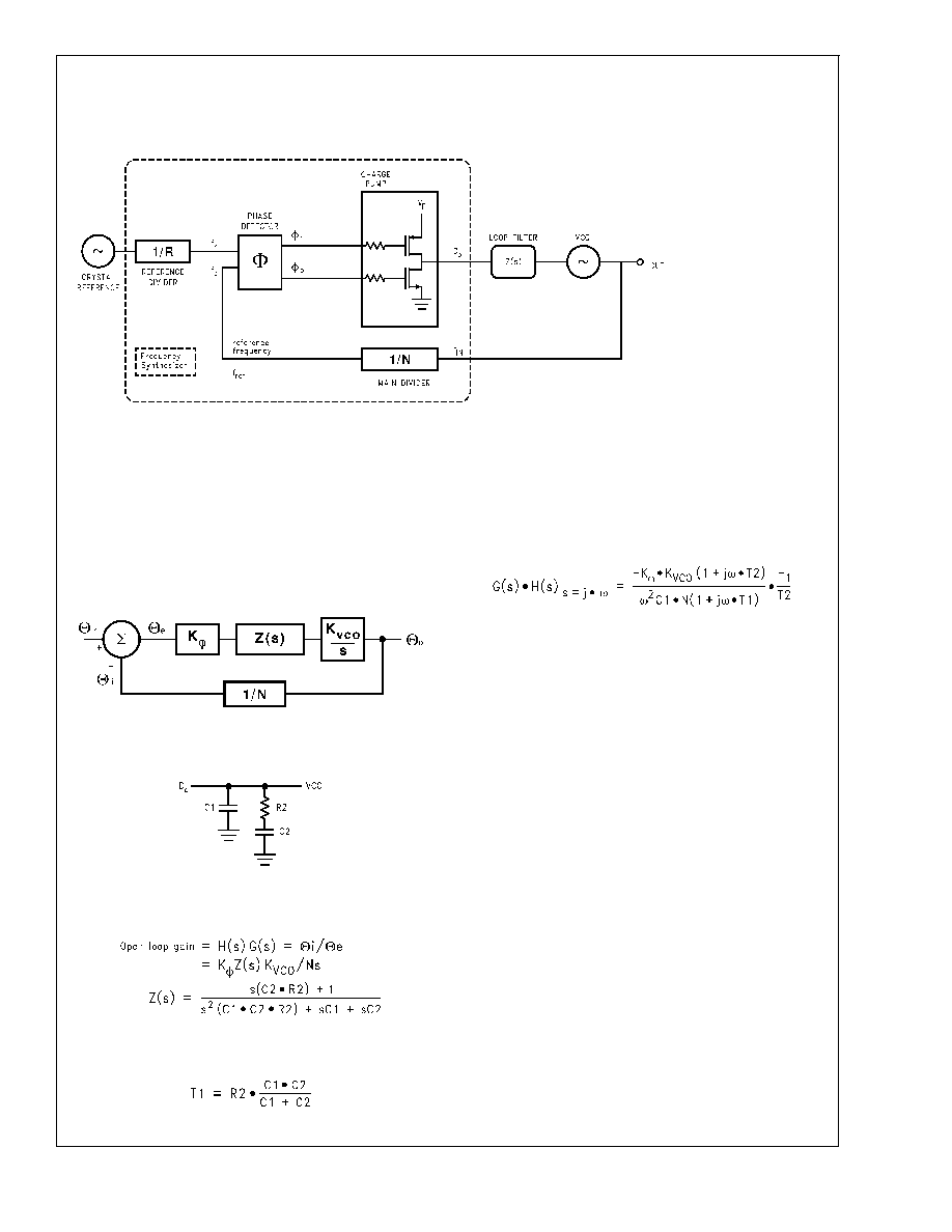
Application Information
A block diagram of the basic phase locked loop is shown in
Figure 1.
LOOP GAIN EQUATIONS
A linear control system model of the phase feedback for a
PLL in the locked state is shown in
Figure 2. The open loop
gain is the product of the phase comparator gain (K
), the
VCO gain (K
VCO
/s), and the loop filter gain Z(s) divided by
the gain of the feedback counter modulus (N). The passive
loop filter configuration used is displayed in
Figure 3, while
the complex impedance of the filter is given in
Equation (1).
(1)
The time constants which determine the pole and zero fre-
quencies of the filter transfer function can be defined as
(2)
and
T2 = R2
∑
C2
(3)
The 3rd order PLL Open Loop Gain can be calculated in
terms of frequency,
, the filter time constants T1 and T2,
and the design constants K
, K
VCO
, and N.
(4)
From
Equations (2), (3) we can see that the phase term will
be dependent on the single pole and zero such that the
phase margin is determined in
Equation (5).
(
) = tan
-1
(
∑
T2) - tan
-1
(
∑
T1) + 180∞
(5)
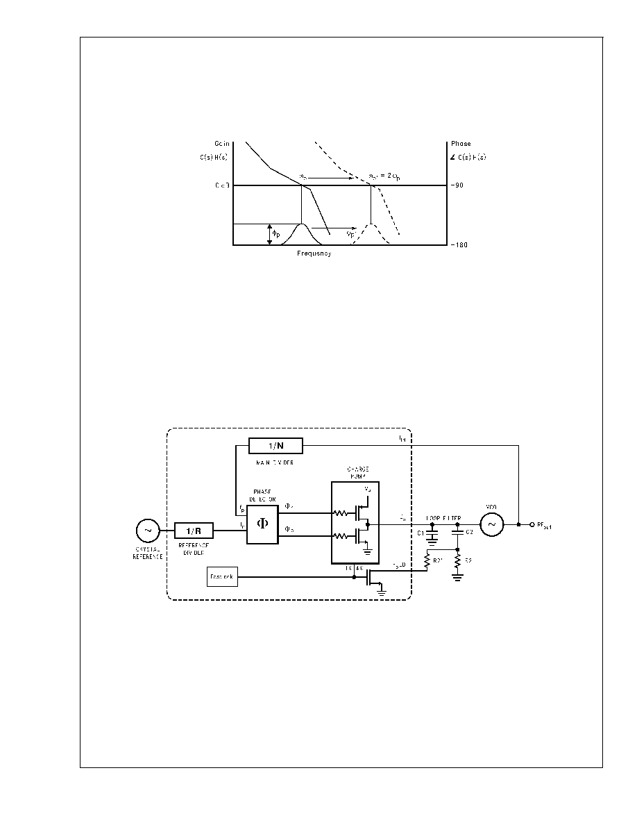
A plot of the magnitude and phase of G(s)H(s) for a stable
loop, is shown in
Figure 4 with a solid trace. The parameter
p
shows the amount of phase margin that exists at the point
the gain drops below zero (the cutoff frequency wp of the
loop). In a critically damped system, the amount of phase
margin would be approximately 45 degrees.
If we were now to redefine the cut off frequency, wp', as
double the frequency which gave us our original loop band-
width, wp, the loop response time would be approximately
halved. Because the filter attenuation at the comparison
frequency also diminishes, the spurs would have increased
by approximately 6 dB. In the proposed Fastlock scheme,
the higher spur levels and wider loop filter conditions would
exist only during the initial lock-on phase -- just long enough
to reap the benefits of locking faster. The objective would be
to open up the loop bandwidth but not introduce any addi-
tional complications or compromises related to our original
design criteria. We would ideally like to momentarily shift the
curve of
Figure 4 over to a different cutoff frequency, illus-
trated by the dotted line, without affecting the relative open
loop gain and phase relationships. To maintain the same
gain/phase relationship at twice the original cutoff frequency,
other terms in the gain and phase
Equation (4) and Equation
(5) will have to compensate by the corresponding "1/w" or
"1/w
2
" factor. Examination of equations
Equations (2), (3)
and
Equation (5) indicates the damping resistor variable R2
could be chosen to compensate the "w"' terms for the phase
01280614
FIGURE 1. Basic Charge Pump Phase Locked Loop
01280615
FIGURE 2. PLL Linear Model
01280616
FIGURE 3. Passive Loop Filter
LMX2330L/LMX2331L/LMX2332L
www.national.com
19
Application Information
(Continued)
margin. This implies that another resistor of equal value to
R2 will need to be switched in parallel with R2 during the
initial lock period. We must also insure that the magnitude of
the open loop gain, H(s)G(s) is equal to zero at wp' = 2wp.
K
vco
, K
, N, or the net product of these terms can be
changed by a factor of 4, to counteract the w
2
term present
in the denominator of
Equation (2) and Equation (3). The K
term was chosen to complete the transformation because it
can readily be switched between 1X and 4X values. This is
accomplished by increasing the charge pump output current
from 1 mA in the standard mode to 4 mA in Fastlock.
FASTLOCK CIRCUIT IMPLEMENTATION
A diagram of the Fastlock scheme as implemented in Na-
tional Semiconductors LMX233XL PLL is shown in
Figure 5.
When a new frequency is loaded, and the RF Icp
o
bit is set
high the charge pump circuit receives an input to deliver 4
times the normal current per unit phase error while an open
drain NMOS on chip device switches in a second R2 resistor
element to ground. The user calculates the loop filter com-
ponent values for the normal steady state considerations.
The device configuration ensures that as long as a second
identical damping resistor is wired in appropriately, the loop
will lock faster without any additional stability considerations
to account for. Once locked on the correct frequency, the
user can return the PLL to standard low noise operation by
sending a MICROWIRE instruction with the RF Icp
o
bit set
low. This transition does not affect the charge on the loop
filter capacitors and is enacted synchronous with the charge
pump output. This creates a nearly seamless change be-
tween Fastlock and standard mode.
01280617
FIGURE 4. Open Loop Response Bode Plot
01280618
FIGURE 5. Fastlock PLL Architecture
LMX2330L/LMX2331L/LMX2332L
www.national.com
20
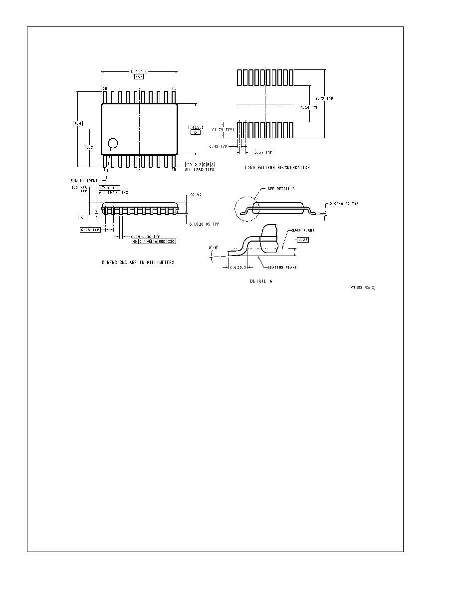
Physical Dimensions
inches (millimeters)
unless otherwise noted
20-Lead (0.173" Wide) Thin Shrink Small Outline Package (TM)
Order Number LMX2330LTM, LMX2331LTM or LMX2332LTM
*
For Tape and Reel (2500 units per reel)
Order Number LMX2330LTMX, LMX2331LTMX or LMX2332LTMX
NS Package Number MTC20
LMX2330L/LMX2331L/LMX2332L
www.national.com
21

Physical Dimensions
inches (millimeters) unless otherwise noted (Continued)
24-Pin Chip Scale Package
For Tape and Reel (2500 Units per Reel)
Order Number LMX2330LSLBX, LMX2331LSLBX or LMX2332LSLBX
NS Package Number SLB24A
LMX2330L/LMX2331L/LMX2332L
www.national.com
22

Physical Dimensions
inches (millimeters) unless otherwise noted (Continued)
20-Pin Thin Chip Scale Package (SLD)
Order Number LMX2330LSLDX, LMX2331LSLDX or LMX2332LSLDX
NS Package Number SLD20A
LIFE SUPPORT POLICY
NATIONAL'S PRODUCTS ARE NOT AUTHORIZED FOR USE AS CRITICAL COMPONENTS IN LIFE SUPPORT
DEVICES OR SYSTEMS WITHOUT THE EXPRESS WRITTEN APPROVAL OF THE PRESIDENT AND GENERAL
COUNSEL OF NATIONAL SEMICONDUCTOR CORPORATION. As used herein:
1. Life support devices or systems are devices or
systems which, (a) are intended for surgical implant
into the body, or (b) support or sustain life, and
whose failure to perform when properly used in
accordance with instructions for use provided in the
labeling, can be reasonably expected to result in a
significant injury to the user.
2. A critical component is any component of a life
support device or system whose failure to perform
can be reasonably expected to cause the failure of
the life support device or system, or to affect its
safety or effectiveness.
National Semiconductor
Corporation
Americas
Email: support@nsc.com
National Semiconductor
Europe
Fax: +49 (0) 180-530 85 86
Email: europe.support@nsc.com
Deutsch Tel: +49 (0) 69 9508 6208
English
Tel: +44 (0) 870 24 0 2171
FranÁais Tel: +33 (0) 1 41 91 8790
National Semiconductor
Asia Pacific Customer
Response Group
Tel: 65-2544466
Fax: 65-2504466
Email: ap.support@nsc.com
National Semiconductor
Japan Ltd.
Tel: 81-3-5639-7560
Fax: 81-3-5639-7507
www.national.com
LMX2330L/LMX2331L/LMX2332L
PLLatinum
Low
Power
Dual
Frequency
Synthesizer
for
RF
Personal
Communications
National does not assume any responsibility for use of any circuitry described, no circuit patent licenses are implied and National reserves the right at any time without notice to change said circuitry and specifications.