LMX2370/LMX2371/LMX2372
PLLatinum
TM
Dual Frequency Synthesizer for RF
Personal Communications
LMX2370
2.5 GHz/1.2 GHz
LMX2371
2.0 GHz/1.2 GHz
LMX2372
1.2 GHz/1.2 GHz
General Description
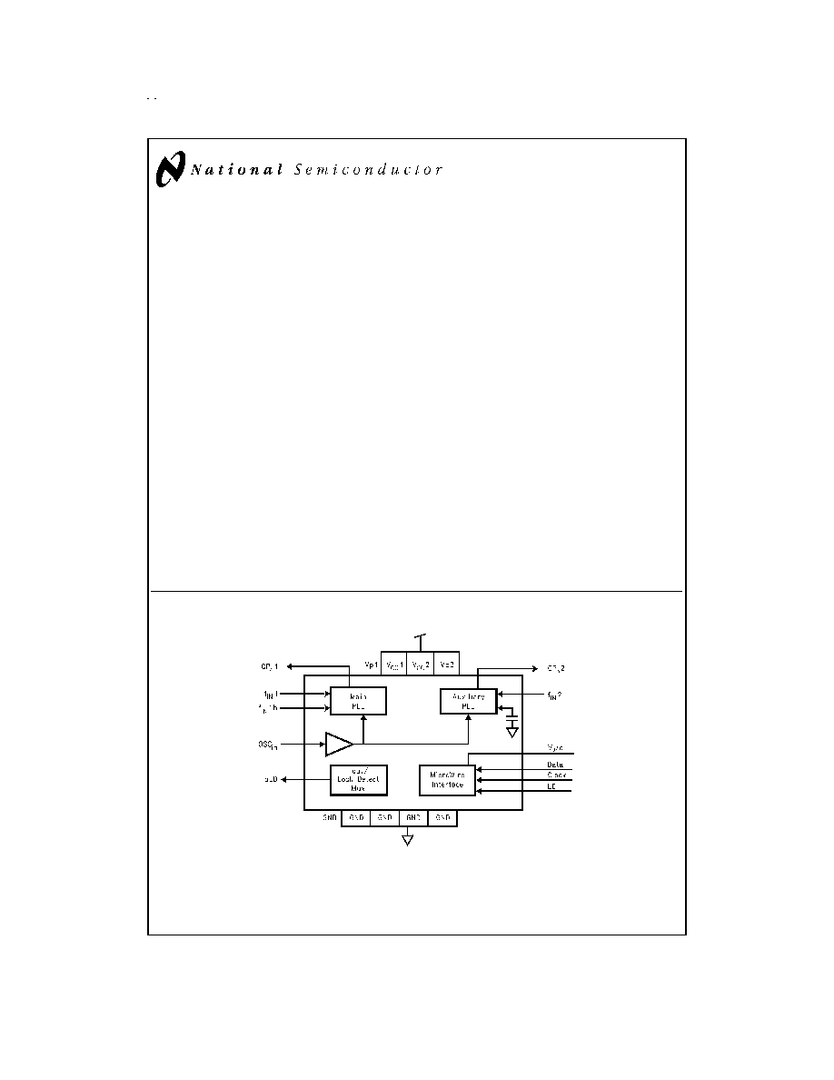
The LMX237X family of monolithic, integrated dual fre-
quency synthesizers, including prescalers, is designed to be
used as a first and second local oscillator for dual mode or
dual conversion transceivers. It is fabricated using National's
0.5u ABiCV silicon BiCMOS process. The LMX237X con-
tains two dual modulus prescalers. A 32/33 or a 16/17
prescaler can be selected for the 2.5 GHz and 2.0 GHz RF
synthesizers with the 16/17 prescaler rated for input frequen-
cies below 1.2 GHz. A 16/17 or an 8/9 prescaler can be se-
lected for the 1.2 GHz RF synthesizers with the 8/9 prescaler
rated for input frequencies below 550 MHz. Using a digital
phase locked loop technique, the LMX237X can generate
very stable, low noise control signals for UHF and VHF volt-
age controlled oscillators (VCO's). Serial data is transferred
into the LMX237X via a 1.8V three wire interface (Data, En-
able, Clock) compatible with low voltage baseband proces-
sors. Supply voltage can range from 2.7V to 5.5V. The
LMX237X family features very low current consumption typi-
cally: LMX2370 - 6.0 mA
@
3V, LMX2371 - 5.0 mA
@
3V,
LMX2372 - 4.0 mA
@
3V.
The LMX237X are available in a 24-pad chip scale (CSP) or
a 20-pin TSSOP surface mount plastic package.
Features
n
2.7V�5.5V operation
n
Ultra low current consumption
n
Low phase detector noise floor
n
Low voltage MICROWIRE
TM
interface (1.8V up to V
CC
)
n
Low prescaler values
32/33
@
f
IN
2.5 GHz
16/17
@
f
IN
1.2 GHz
8/9
@
f
IN
550 MHz
n
Selectable charge pump current levels
n
Selectable FastLock
TM
mode
n
Enhanced ESD protection
n
Small 24 pad chip scale package (3.5 x 4.5 x 1.0 mm)
Applications
n
Portable wireless communications (PCS/PCN, cordless)
n
Dual mode cellular telephone systems
n
Spread spectrum communication systems (CDMA)
n
Cable TV tuners (CATV)
Functional Block Diagram
FastLock
TM
, PLLatinum
TM
and MICROWIRE
TM
are trademarks of National Semiconductor Corporation.
TRI-STATE
�
is a registered trademark of National Semiconductor Corporation.
DS101026-1
PRELIMINARY
March 1999
LMX2370/LMX2371/LMX2372
PLLatinum
Dual
Frequency
Synthesizer
for
RF
Personal
Communications
� 1999 National Semiconductor Corporation
DS101026
www.national.com
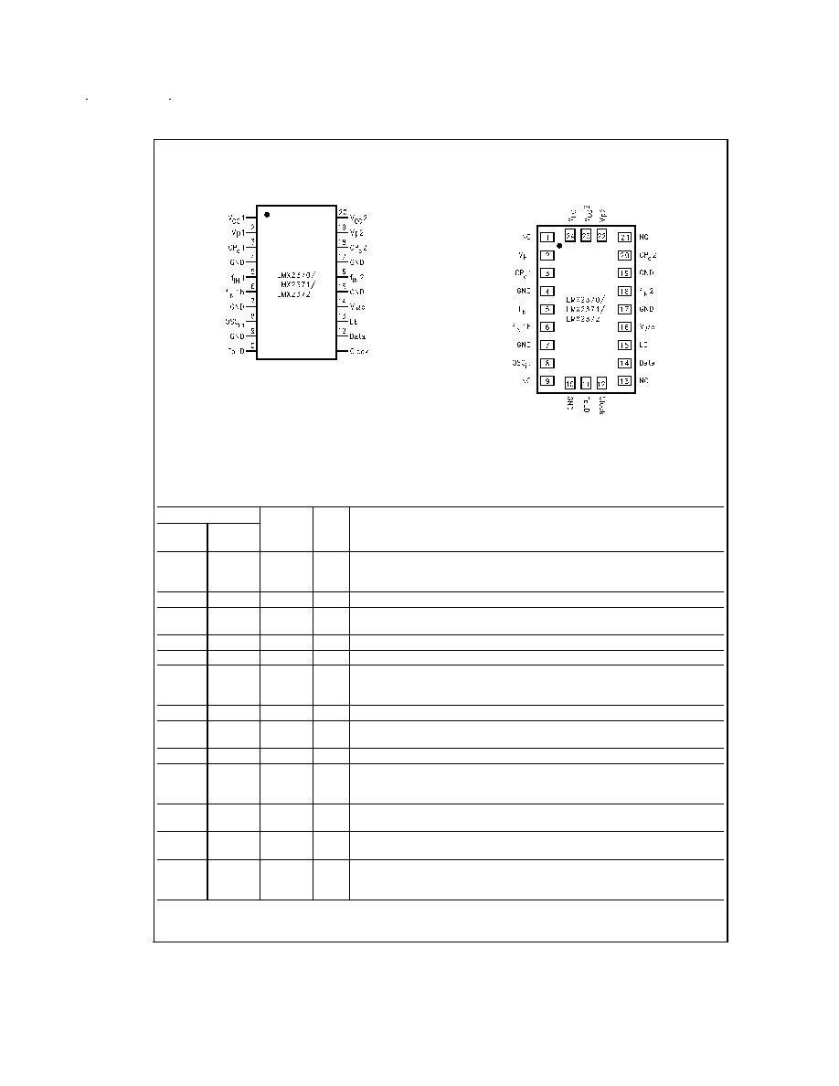
Connection Diagrams
Pin Descriptions
Pin No.
Pin
Name
I/O
Description
24-Pin
CSP
20-Pin
TSSOP
24
1
V
CC
1
--
Power supply voltage input for RF analog and RF digital circuits. Input may range
from 2.7V to 5.5V. V
CC
1 must equal V
CC
2. Bypass capacitors should be placed as
close as possible to this pin and be connected directly to the ground plane.
2
2
Vp1
--
Power supply for Main charge pump. Must be
V
CC
.
3
3
CP
o
1
O
Internal Main charge pump output. For connection to a loop filter for driving the
input of an external VCO.
4
4
GND
--
Ground for Main digital circuitry.
5
5
f
IN
1
I
Main prescaler input. Small signal input from the VCO.
6
6
f
IN
1b
I
Main prescaler complementary input. For single ended operation, a bypass
capacitor should be placed as close as possible to this pin and be connected
directly to the ground plane.
7
7
GND
--
Ground for Main analog circuitry.
8
8
OSC
in
I
Oscillator input. The input has a V
CC
/2 input threshold and can be driven from an
external CMOS or TTL logic gate.
10
9
GND
--
Ground for Aux digital, MICROWIRE, FoLD, and oscillator circuits.
11
10
Fo/LD
O
Multiplexed output of the Main/Aux programmable or reference dividers,
Main/Auxiliary lock detect signals and Fastlock mode. CMOS output
(see
Programmable Modes in the Datasheet).
12
11
Clock
I
High impedance CMOS Clock input. Data for the various counters is clocked in on
the rising edge, into the 22-bit shift register.
14
12
Data
I
Binary serial data input. Data entered MSB first. The last two bits are the control
bits. High impedance CMOS input.
15
13
LE
I
Load enable. High impedance CMOS input. When LE goes HIGH, data stored in
the shift registers is loaded into one of the 4 appropriate latches (control bit
dependent).
TSSOP 20-Pin Package
DS101026-2
Top View
Order Number LMX2370TM, LMX2370TMX,
LMX2371TM, LMX2371TMX,
LMX2372TM or LMX2372TMX
See NS Package Number MTC20
CSP 24-Pin Package
DS101026-3
Top View
Order Number LMX2370SLBX,
LMX2371SLBX or LMX2372SLBX
See NS Package Number SLB24A
www.national.com
2
Pin Descriptions
(Continued)
Pin No.
Pin
Name
I/O
Description
24-Pin
CSP
20-Pin
TSSOP
16
14
V�c
--
Power supply for MICROWIRE circuitry. Must be
V
CC
. Typically connected to
same supply level as �processor or baseband controller to enable programming at
low voltages.
17
15
GND
--
Ground for Aux analog circuitry.
18
16
f
IN
2
I
Auxiliary prescaler input. Small signal input from the VCO.
19
17
GND
--
Ground for Aux digital, MICROWIRE, FoLD, and oscillator.
20
18
CP
o
2
O
Aux internal charge pump output. For connection to a loop filter for driving the
input of an external VCO.
22
19
Vp2
--
Power supply for Aux charge pump. Must be
V
CC
.
23
20
V
CC
2
--
Power supply voltage input for Aux analog, Aux digital, FoLD, and oscillator
circuits. Input may range from 2.7V to 5.5V. V
CC
2 must equal V
CC
1. Bypass
capacitors should be placed as close as possible to this pin and be connected
directly to the ground plane.
1, 9,
13, 21
--
NC
--
No Connect
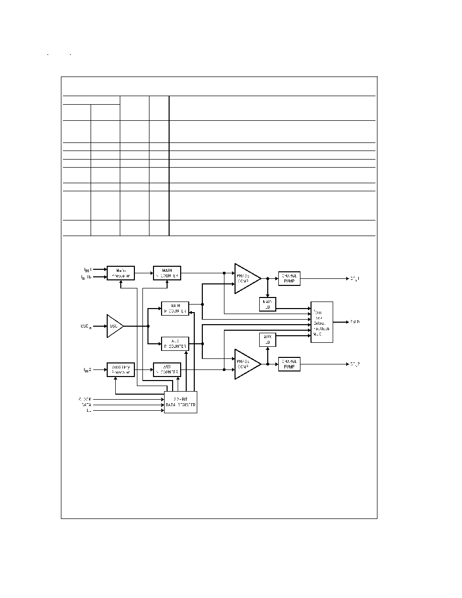
Block Diagram
DS101026-4
www.national.com
3
Absolute Maximum Ratings
(Notes 1, 2)
If Military/Aerospace specified devices are required,
please contact the National Semiconductor Sales Office/
Distributors for availability and specifications.
Power Supply Voltage
V
CC
1
-0.3V to 6.5V
V
CC
2
-0.3V to 6.5V
Vp1
-0.3V to 6.5V
Vp2
-0.3V to 6.5V
V�c
-0.3V to 6.5V
Voltage on any pin with
GND = 0V (V
I
)
-0.3V to V
CC
+0.3V
Storage Temperature Range (T
S
)
-65�C to +150�C
Lead Temperature (solder, 4 sec.) (T
L
)
+260�C
ESD - Human Body Model (Note 2)
TBD
Recommended Operating
Conditions
(Note 3)
Power Supply Voltage
V
CC
1
2.7V to 5.5V
V
CC
2
2.7V to 5.5V
V
CC
1�V
CC
2
-0.2V to 0.2V
Vp1
V
CC
to 5.5V
Vp2
V
CC
to 5.5V
V�c
1.72V to V
CC
Operating Temperature (T
A
)
-40�C to +85�C
Note 1: Absolute Maximum Ratings indicate limits beyond which damage to
the device may occur. Operating Ratings indicate conditions for which the de-
vice is intended to be functional, but do not guarantee specific performance
limits. For guaranteed specifications and test conditions, see the Electrical
Characteristics. The guaranteed specifications apply only for the test condi-
tions listed.
Note 2: This device is a high performance RF integrated circuit and is ESD
sensitive. Handling and assembly of this device should only be done at ESD
free workstations.
Note 3: V
CC
is defined as V
CC
= V
CC
1 = V
CC
2.
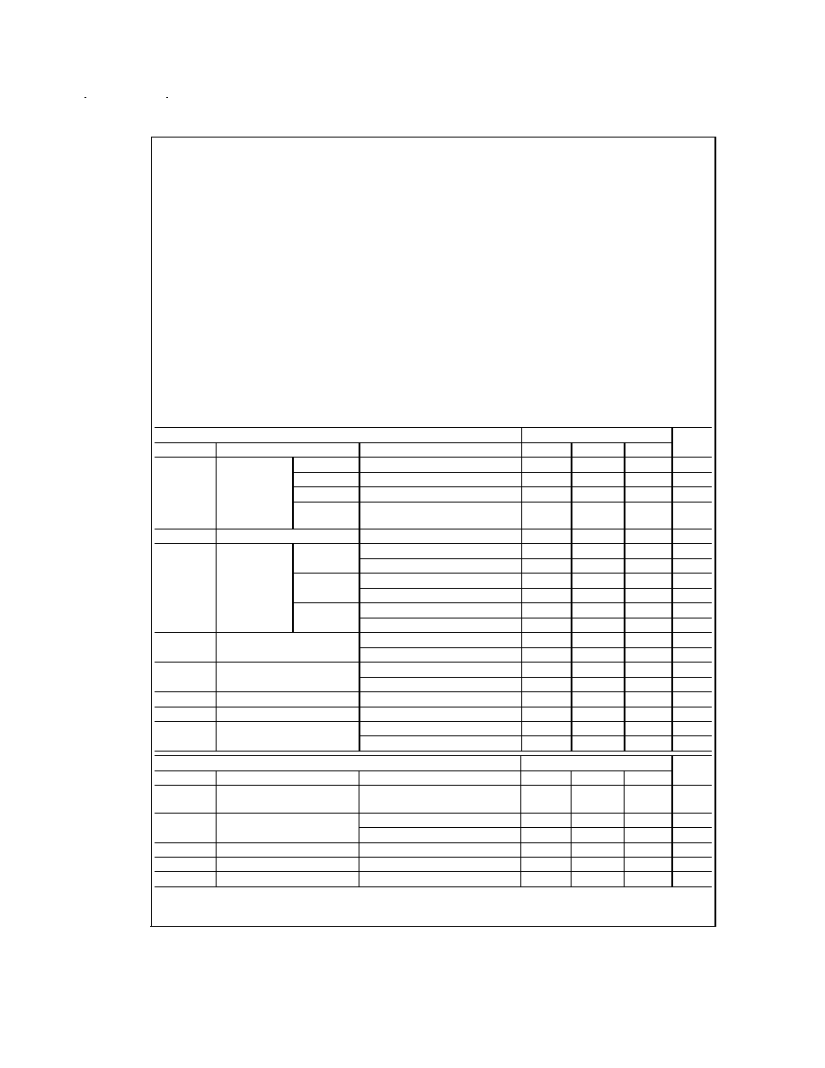
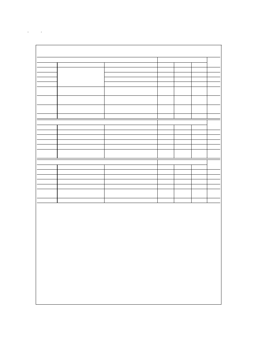
Electrical Characteristics
(V
CC
= Vp = V�c = 3.0V; -40�C
<
T
A
<
85�C except as specified).
GENERAL
Value
Unit
Symbol
Parameter
Conditions
Min
Typ
Max
I
CC
Power Supply
Current
LMX2370
Main = On, Aux = On
6
8.5
mA
LMX2371
Main = On, Aux = On
5
7.5
mA
LMX2372
Main = On, Aux = On
4
6.0
mA
LMX2370
/71/72
Aux Only
2
3.25
mA
I
CC-PWDN
Power Down Current
EN_Main, EN_Aux = 0
15
50
�A
f
IN
1
Main PLL
Operating
Frequency
LMX2370
P = 32/33
1.2
2.5
GHz
P = 16/17
45
1200
MHz
LMX2371
P = 32/33
1.2
2.0
GHz
P = 16/17
45
1200
MHz
LMX2372
P = 16/17
45
1200
MHz
P = 8/9
45
550
MHz
f
IN
2
Auxiliary PLL Operating
Frequency
P = 16/17
45
1200
MHz
P = 8/9
45
550
MHz
Zf
IN
Main
Main PLL Input Impedance
RF On, f
IN
= 1800 MHz
TBD
RF Off, f
IN
= 1800 MHz
TBD
Zf
IN
Aux
Aux Input Impedance
f
IN
= 120 MHz
TBD
f
Phase Detector Frequency
10
MHz
Pf
IN
1, Pf
IN
2
RF Input Sensitivity
2.7
V
CC
3.6V
-15
0
dBm
3.6
V
CC
5.5V
-10
0
dBm
OSCILLATOR INPUT
Value
Unit
Symbol
Parameter
Conditions
Min
Typ
Max
OSC
in
Reference Oscillator Input
Operating Frequency
2
50
MHz
Z
IN
OSC
OSC Input Impedance
OSC On, Freq = 10 MHz
TBD
k
OSC Off, Freq = 10 MHz
TBD
k
V
OSC
Oscillator Input Sensitivity
OSC
in
0.5
V
CC
V
PP
I
IH
OSC
in
Input Current
V
IH
= V
CC
= 5.5V
100
�A
I
IL
OSC
in
Input Current
V
IL
= 0, V
CC
= 5.5V
-100
�A
www.national.com
4
Electrical Characteristics
(V
CC
= Vp = V�c = 3.0V; -40�C
<
T
A
<
85�C except as specified). (Continued)
CHARGE PUMP
Value
Unit
Symbol
Parameter
Conditions
Min
Typ
Max
ICP
o-source
Main and Auxiliary Charge
Pump Output Current (Note 4)
VCP
o
= Vp/2, ICP
o
_4X = 0
1.0
mA
ICP
o-sink
VCP
o
= Vp/2, ICP
o
_4X = 0
-1.0
mA
ICP
o-source
VCP
o
= Vp/2, ICP
o
_4X = 1
4.0
mA
ICP
o-sink
VCP
o
= Vp/2, ICP
o
_4X = 1
-4.0
mA
ICP
o-TRI
Charge Pump TRI-STATE
�
Current
0.5
VCP
o
Vp - 0.5,
-40�C
<
T
A
<
85�C
-2.5
0.1
2.5
nA
ICP
o-sink
vs
ICP
o-source
CP Sink vs Source Mismatch
VCP
o
= Vp/2, T
A
= 25�C
3
10
%
ICP
o
vs
VCP
o
CP Current vs Voltage
0.5
VCP
o
Vp - 0.5, T
A
= 25�C
8
15
%
ICP
o
vs T
A
CP Current vs Temperature
VCP
o
= Vp/2, -40�C
<
T
A
<
85�C
8
%
DIGITAL INTERFACE (DATA, CLOCK, LE)
Value
Unit
Symbol
Parameter
Conditions
Min
Typ
Max
V
IH
High-Level Input Voltage
V�c = 1.72V to 5.5V
0.8 V�c
V
V
IL
Low-Level Input Voltage
V�c = 1.72V to 5.5V
0.2 V�c
V
I
IH
High-Level Input Current
V
IH
= V�c = 5.5V
-1.0
1.0
�A
I
IL
Low-Level Input Current
V
IL
= 0, V�c = 5.5V
-1.0
1.0
�A
V
OL
Low-Level Output Current
I
OL
= 1.0 mA, V
EXT
= 1.8V (Note
5)
0.1
0.4
V
MICROWIRE TIMING
Value
Unit
Symbol
Parameter
Conditions
Min
Typ
Max
t
CS
Data to Clock Setup Time
See Data Input Timing
50
ns
t
CH
Data to Clock Hold Time
See Data Input Timing
20
ns
t
CWH
Clock Pulse Width High
See Data Input Timing
50
ns
t
CWL
Clock Pulse Width Low
See Data Input Timing
50
ns
t
ES
Clock to Load Enable Setup
Time
See Data Input Timing
50
ns
t
EW
Load Enable Pulse Width
See Data Input Timing
50
ns
Note 4: Main and Auxiliary Charge Pump magnitude are controlled by Main_ICP
o
_4X and Aux_ICP
o
_4X bits respectively.
Note 5: Lock Detect open drain output only pulled up to V
EXT
. Typically V
EXT
= V
CC
.
1.0 Functional Description
The basic phase-lock-loop (PLL) configuration consists of a high-stability crystal reference oscillator, a frequency synthesizer
such as the National Semiconductor LMX2370/2371/2372, a voltage controlled oscillator (VCO), and a passive loop filter. The fre-
quency synthesizer includes a phase detector, a current mode charge pump, as well as programmable reference [R] and feed-
back [N] frequency dividers. The VCO frequency is established by dividing the crystal reference signal down via the R-counter to
obtain a comparison reference frequency. This reference signal (
f
R
) is then presented to the input of a phase/frequency detector
and compared with the feedback signal (
f
N
), which is obtained by dividing the VCO frequency down by way of the N-counter. The
phase/frequency detector's current source output pumps charge into the loop filter, which then integrates into the VCO's control
voltage. The function of the phase/frequency comparator is to adjust the control voltage presented to the VCO until the feedback
signal frequency and phase match that of the reference signal. When this "Phase-Locked" condition exists, the VCO frequency
will be N times that of the comparison frequency, where N is the integer divide ratio.
1.1 REFERENCE OSCILLATOR INPUT
The reference oscillator frequency for the Main and Auxiliary PLLs is provided from the external reference through the OSC
in
pin.
OSC
in
can operate up to 50 MHz with input sensitivity of 0.5 V
PP
. The OSC
in
pin drives both the Main R-counter and the Auxiliary
R-counter. The input has a V
CC
/2 input threshold that can be driven from an external CMOS or TTL logic gate. Typically, the OSC
in
is connected to the output of a crystal oscillator.
1.2 REFERENCE DIVIDERS (R-COUNTERS)
The Main and Auxiliary R-counters are both clocked through the oscillator block in common. The maximum frequency is 50 MHz.
Both R-counters are CMOS design and 15-bit in length with programmable divider ratio from 2 to 32,767.
www.national.com
5