 | ÐлекÑÑоннÑй компоненÑ: LMX2487 | СкаÑаÑÑ:  PDF PDF  ZIP ZIP |
Äîêóìåíòàöèÿ è îïèñàíèÿ www.docs.chipfind.ru
LMX2487
3.0 GHz - 6.0 GHz High Performance Delta-Sigma Low
Power Dual PLLatinum
TM
Frequency Synthesizers with
3.0 GHz Integer PLL
General Description
The LMX2487 is a low power, high performance delta-sigma
fractional-N PLL with an auxiliary integer-N PLL. It is fabri-
cated using National Semiconductor's advanced process.
With delta-sigma architecture, fractional spurs at lower offset
frequencies are pushed to higher frequencies outside the
loop bandwidth. The ability to push close in spur and phase
noise energy to higher frequencies is a direct function of the
modulator order. Unlike analog compensation, the digital
feedback technique used in the LMX2487 is highly resistant
to changes in temperature and variations in wafer process-
ing. The LMX2487 delta-sigma modulator is programmable
up to fourth order, which allows the designer to select the
optimum modulator order to fit the phase noise, spur, and
lock time requirements of the system.
Serial data for programming the LMX2487 is transferred via
a three line high speed (20 MHz) MICROWIRE interface.
The LMX2487 offers fine frequency resolution, low spurs,
fast programming speed, and a single word write to change
the frequency. This makes it ideal for direct digital modula-
tion applications, where the N counter is directly modulated
with information. The LMX2487 is available in a 24 lead
4.0 X 4.0 X 0.8 mm LLP package.
Applications
n
Cellular phones and base stations
n
Direct digital modulation applications
n
Satellite and cable TV tuners
n
WLAN Standards
Features
Quadruple Modulus Prescalers for Lower Divide Ratios
n
RF PLL: 16/17/20/21 or 32/33/36/37
n
IF PLL: 8/9 or 16/17
Advanced Delta Sigma Fractional Compensation
n
12 bit or 22 bit selectable fractional modulus
n
Up to 4th order programmable delta-sigma modulator
Features for Improved Lock Times and Programming
n
Fastlock / Cycle slip reduction
n
Integrated time-out counter
n
Single word write to change frequencies with Fastlock
Wide Operating Range
n
LMX2487 RF PLL: 3.0 GHz to 6.0 GHz
Useful Features
n
Digital lock detect output
n
Hardware and software power-down control
n
On-chip crystal reference frequency doubler.
n
RF phase comparison frequency up to 50 MHz
n
2.5 to 3.6 volt operation with I
CC
= 8.5 mA at 3.0 V
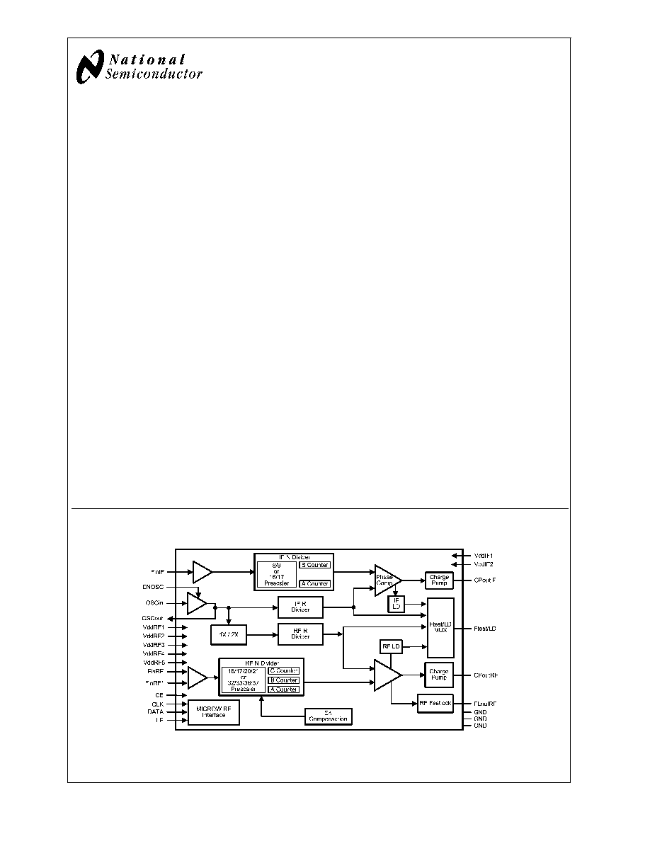
Functional Block Diagram
20154701
PLLatinum
TM
is a trademark of National Semiconductor Corporation.
February 2006
LMX2487
High
Performance
Delta-Sigma
Low
Power
Dual
PLLatinum
Frequency
Synthesizer
© 2006 National Semiconductor Corporation
DS201547
www.national.com
Connection Diagram
Top View
24-Pin LLP (SQ)
20154722
Pin Descriptions
Pin #
Pin
Name
I/O
Pin Description
0
GND
-
Ground Substrate. This is on the bottom of the package and must be grounded.
1
CPoutRF
O
RF PLL charge pump output.
2
GND
-
RF PLL analog ground.
3
VddRF1
-
RF PLL analog power supply.
4
FinRF
I
RF PLL high frequency input pin.
5
FinRF*
I
RF PLL complementary high frequency input pin. Shunt to ground with a 100 pF
capacitor.
6
LE
I
MICROWIRE Load Enable. High impedance CMOS input. Data stored in the shift
registers is loaded into the internal latches when LE goes HIGH
7
DATA
I
MICROWIRE Data. High impedance binary serial data input.
8
CLK
I
MICROWIRE Clock. High impedance CMOS Clock input. Data for the various counters is
clocked into the 24 bit shift register on the rising edge
9
VddRF2
-
Power supply for RF PLL digital circuitry.
10
CE
I
Chip Enable control pin. Must be pulled high for normal operation.
11
VddRF5
I
Power supply for RF PLL digital circuitry.
12
Ftest/LD
O
Test frequency output / Lock Detect.
13
FinIF
I
IF PLL high frequency input pin.
14
VddIF1
-
IF PLL analog power supply.
15
GND
-
IF PLL digital ground.
16
CPoutIF
O
IF PLL charge pump output
17
VddIF2
-
IF PLL power supply.
18
OSCout
O
Buffered output of the OSCin signal.
19
ENOSC
I
Oscillator enable. When this is set to high, the OSCout pin is enabled regardless of the
state of other pins or register bits.
20
OSCin
I
Reference Input.
21
NC
I
This pin must be left open.
22
VddRF3
-
Power supply for RF PLL digital circuitry.
23
FLoutRF
O
RF PLL Fastlock Output. Also functions as Programmable TRI-STATE CMOS output.
24
VddRF4
-
RF PLL analog power supply.
LMX2487
www.national.com
2
Absolute Maximum Ratings
(Notes 1, 2)
Parameter
Symbol
Value
Units
Min
Typ
Max
Power Supply Voltage
V
CC
-0.3
4.25
V
Voltage on any pin with GND = 0V
V
i
-0.3
V
CC
+0.3
V
Storage Temperature Range
T
s
-65
+150
°C
Lead Temperature (Solder 4 sec.)
T
L
+260
°C
Recommended Operating Conditions
Parameter
Symbol
Value
Units
Min
Typ
Max
Power Supply Voltage (Note 1)
V
CC
2.5
3.0
3.6
V
Operating Temperature
T
A
-40
25
+85
°C
Note 1: "Absolute Maximum Ratings" indicate limits beyond which damage to the device may occur. "Recommended Operating Conditions" indicate conditions for
which the device is intended to be functional, but do not guarantee specific performance limits. For guaranteed specifications and test conditions, see the Electrical
Characteristics. The guaranteed specifications apply only for the test conditions listed. The voltage at all the power supply pins of VddRF1, VddRF2, VddRF3,
VddRF4, VddRF5, VddIF1 and VddIF2 must be the same. V
CC
will be used to refer to the voltage at these pins and I
CC
will be used to refer to the sum of all currents
through all these power pins.
Note 2: This Device is a high performance RF integrated circuit with an ESD rating
<
2 kV and is ESD sensitive. Handling and assembly of this device should only
be done at ESD-free workstations.
Electrical Characteristics
(V
CC
= 3.0V; -40°C
T
A
+85°C unless otherwise specified)
Symbol
Parameter
Conditions
Value
Units
Min
Typ
Max
Icc PARAMETERS
I
CC
RF
Power Supply Current,
RF Synthesizer
IF PLL OFF
RF PLL ON
Charge Pump TRI-STATE
5.7
mA
I
CC
IF
Power Supply Current,
IF Synthesizer
IF PLL ON
RF PLL OFF
Charge Pump TRI-STATE
2.5
mA
I
CC
TOTAL
Power Supply Current,
Entire Synthesizer
IF PLL ON
RF PLL ON
Charge Pump TRI-STATE
8.5
mA
I
CC
PD
Power Down Current
CE = ENOSC = 0V
CLK, DATA, LE = 0V
<
1
µA
RF SYNTHESIZER PARAMETERS
f
FinRF
Operating
Frequency
LMX2487
RF_P = 16
3000
4000
MHz
RF_P = 32
3000
6000
p
FinRF
Input Sensitivity
3000 - 6000 MHz
-10
0
dBm
f
COMP
Phase Detector
Frequency
(Note 3)
50
MHz
I
CPoutRF
SRCE
RF Charge Pump
Source Current
(Note 4)
RF_CPG = 0
V
CPoutRF
= V
CC
/2
95
µA
RF_CPG = 1
V
CPoutRF
= V
CC
/2
190
µA
...
...
µA
RF_CPG = 15
V
CPoutRF
= V
CC
/2
1520
µA
LMX2487
www.national.com
3
Electrical Characteristics
(V
CC
= 3.0V; -40°C
T
A
+85°C unless otherwise specified) (Continued)
Symbol
Parameter
Conditions
Value
Units
Min
Typ
Max
RF SYNTHESIZER PARAMETERS
I
CPoutRF
SINK
RF Charge Pump Sink
Current
(Note 4)
RF_CPG = 0
V
CPoutRF
= V
CC
/2
-95
µA
RF_CPG = 1
V
CPoutRF
= V
CC
/2
-190
µA
...
...
µA
RF_CPG = 15
V
CPoutRF
= V
CC
/2
-1520
µA
I
CPoutRF
TRI
RF Charge Pump
TRI-STATE Current
Magnitude
0.5
V
CPoutRF
V
CC
-0.5
2
10
nA
| I
CPoutRF
%MIS |
Magnitude of RF CP
Sink vs. CP Source
Mismatch
V
CPoutRF
=
V
CC
/2
T
A
= 25°C
RF_CPG
>
2
3
10
%
RF_CPG
2
3
13
%
| I
CPoutRF
%V |
Magnitude of RF CP
Current vs. CP Voltage
0.5
V
CPoutRF
V
CC
-0.5
T
A
= 25°C
2
8
%
| I
CPoutRF
%T |
Magnitude of RF CP
Current vs. Temperature
V
CPoutRF
= V
CC
/2
4
%
IF SYNTHESIZER PARAMETERS
f
FinIF
Operating Frequency
IF_P = 8
250
2000
MHz
IF_P = 16
250
3000
p
FinIF
IF Input Sensitivity
-10
+5
dBm
f
COMP
Phase Detector
Frequency
10
MHz
I
CPoutIF
SRCE
IF Charge Pump Source
Current
V
CPoutIF
= V
CC
/2
3.5
mA
I
CPoutIF
SINK
IF Charge Pump Sink
Current
V
CPoutIF
= V
CC
/2
-3.5
mA
I
CPoutIF
TRI
IF Charge Pump
TRI-STATE Current
Magnitude
0.5
V
CPoutIF
V
CC
RF -0.5
2
10
nA
| I
CPoutIF
%MIS |
Magnitude of IF CP Sink
vs. CP Source Mismatch
V
CPoutIF
= V
CC
/2
T
A
= 25°C
1
8
%
| I
CPoutIF
%V |
Magnitude of IF CP
Current vs. CP Voltage
0.5
V
CPoutIF
V
CC
-0.5
T
A
= 25°C
4
10
%
| I
CPoutIF
%TEMP
Magnitude of IF CP
Current vs. Temperature
V
CPoutIF
= V
CC
/2
4
%
OSCILLATOR PARAMETERS
f
OSCin
Oscillator Operating
Frequency
OSC2X = 0
5
110
MHz
OSC2X = 1
5
20
MHz
v
OSCin
Oscillator Input
Sensitivity
0.5
V
CC
V
P-P
I
OSCin
Oscillator Input Current
-100
100
µA
SPURS
Spurs in band(Note 5)
-55
dBc
LMX2487
www.national.com
4
Electrical Characteristics
(V
CC
= 3.0V; -40°C
T
A
+85°C unless otherwise specified) (Continued)
Symbol
Parameter
Conditions
Value
Units
Min
Typ
Max
PHASE NOISE
L
F1Hz
RF
RF Synthesizer
Normalized Phase Noise
Contribution(Note 6)
RF_CPG = 0
-202
dBc/Hz
RF_CPG = 1
-204
RF_CPG = 3
-206
RF_CPG = 7
-210
RF_CPG = 15
-210
L
F1Hz
IF
IF Synthesizer
Normalized Phase Noise
Contribution
-209
dBc/Hz
DIGITAL INTERFACE (DATA, CLK, LE, ENOSC, CE, Ftest/LD, FLoutRF)
V
IH
High-Level Input Voltage
1.6
V
CC
V
V
IL
Low-Level Input Voltage
0.4
V
I
IH
High-Level Input Current V
IH
= V
CC
-1.0
1.0
µA
I
IL
Low-Level Input Current
V
IL
= 0 V
-1.0
1.0
µA
V
OH
High-Level Output
Voltage
I
OH
= -500 µA
V
CC
-0.4
V
V
OL
Low-Level Output
Voltage
I
OL
= 500 µA
0.4
V
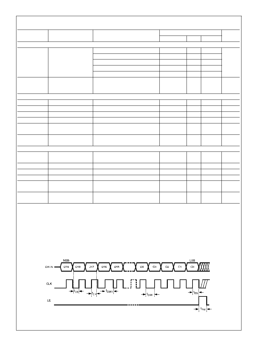
MICROWIRE INTERFACE TIMING
t
CS
Data to Clock Set Up
Time
See MICROWIRE Input Timing
25
ns
t
CH
Data to Clock Hold Time See MICROWIRE Input Timing
8
ns
t
CWH
Clock Pulse Width High
See MICROWIRE Input Timing
25
ns
t
CWL
Clock Pulse Width Low
See MICROWIRE Input Timing
25
ns
t
ES
Clock to Load Enable
Set Up Time
See MICROWIRE Input Timing
25
ns
t
EW
Load Enable Pulse
Width
See MICROWIRE Input Timing
25
ns
Note 3: For Phase Detector Frequencies above 20 MHz, Cycle Slip Reduction (CSR) may be required. Legal divide ratios are also required.
Note 4: Refer to table in Section 2.4.2 RF_CPG -- RF PLL Charge Pump Gain for complete listing of charge pump currents.
Note 5: In order to measure the in-band spur, the fractional word is chosen such that when reduced to lowest terms, the fractional numerator is one. The spur offset
frequency is chosen to be the comparison frequency divided by the reduced fractional denominator. The loop bandwidth must be sufficiently wide to negate the
impact of the loop filter. Measurement conditions are: Spur Offset Frequency = 10 kHz, Loop Bandwidth = 100 kHz, Fraction = 1/2000, Comparison Frequency =
20 MHz, RF_CPG = 7, DITH = 0, VCO Frequency = 3 GHz, and a 4th Order Modulator (FM = 0). These are relatively consistent over tuning range.
Note 6: Normalized Phase Noise Contribution is defined as: L
N
(f) = L(f) 20log(N) 10log(f
COMP
) where L(f) is defined as the single side band phase noise
measured at an offset frequency, f, in a 1 Hz Bandwidth. The offset frequency, f, must be chosen sufficiently smaller than the PLL loop bandwidth, yet large enough
to avoid substantial phase noise contribution from the reference source. Measurement conditions are: Offset Frequency = 11 kHz, Loop Bandwidth = 100 kHz for
RF_CPG = 7, Fraction = 1/2000, Comparison Frequency = 20 MHz, FM = 0, DITH = 0, VCO Frequency = 3 GHz.
MICROWIRE INPUT TIMING DIAGRAM
20154775
LMX2487
www.national.com
5
Document Outline