LMX2531
PLLatinum
TM
High Performance Frequency Synthesizer
System with Integrated VCO
General Description
The LMX2531 is a low power, high performance frequency
synthesizer system which includes a fully integrated delta-
sigma PLL and VCO with fully integrated tank circuit. The
third and fourth poles are also integrated and also adjust-
able. Also included are integrated ultra-low noise and high
precision LDOs for the PLL and VCO which give higher
supply noise immunity and also more consistent perfor-
mance. When combined with a high quality reference oscil-
lator, the LMX2531 generates very stable, low noise local
oscillator signals for up and down conversion in wireless
communication devices. The LMX2531 is a monolithic inte-
grated circuit, fabricated in an advanced BiCMOS process.
There are actually several different versions of this product,
for which the primary difference is frequency range.
Device programming is facilitated using a three-wire
MICROWIRE Interface that can operate down to 1.8 volts.
Supply voltage range is 2.8 to 3.2 Volts. The LMX2531 is
available in a 36 pin 6x6x0.8 mm Lead-Free Leadless Lead-
frame Package (LLP).
Target Applications
n
3G Cellular Base Stations (WCDMA,
TD-SCDMA,CDMA2000)
n
2G Cellular Base Stations (GSM/GPRS, EDGE,
CDMA1xRTT)
n
Wireless LAN
n
Broadband Wireless Access
n
Satellite Communications
n
Wireless Radio
n
Automotive
n
CATV Equipment
n
Instrumentation and Test Equipment
n
RFID Readers
Features
Multiple Frequency Options Available
-- See Selection Guide Below
-- Frequencies from: 765 MHz - 2790 MHz
PLL Features
-- Fractional-N Delta Sigma Modulator Order
programmable up to 4th order
-- FastLock/Cycle Slip Reduction with Timeout Counter
-- Partially integrated, adjustable Loop Filter
-- Very low phase noise and spurs
VCO Features
-- Integrated tank inductor
-- Low phase noise
Other Features
-- 2.8 V to 3.2 V Operation
-- Low Power-Down Current
-- 1.8V MICROWIRE Support
-- Package: 36 Lead LLP
Part
Low Band
High Band
LMX2531LQ1570E
765 - 818 MHz
1530 - 1636 MHz
LMX2531LQ1650E
795 - 850 MHz
1590 - 1700 MHz
LMX2531LQ1700E
831 - 885 MHz
1662 - 1770 MHz
LMX2531LQ1778E
863 - 920 MHz
1726 - 1840 MHz
LMX2531LQ1910E
917 - 1014 MHz
1834 - 2028 MHz
LMX2531LQ2080E
952 - 1137 MHz
1904 - 2274 MHz
LMX2531LQ2265E 1089 - 1200 MHz 2178 - 2400 MHz
LMX2531LQ2570E 1168 - 1395 MHz 2336 - 2790 MHz
PLLatinum
TM
is a trademark of National Semiconductor Corporation.
October 2005
LMX2531
High
Performance
Frequency
Synthesizer
System
with
Integrated
VCO
© 2005 National Semiconductor Corporation
DS201011
www.national.com
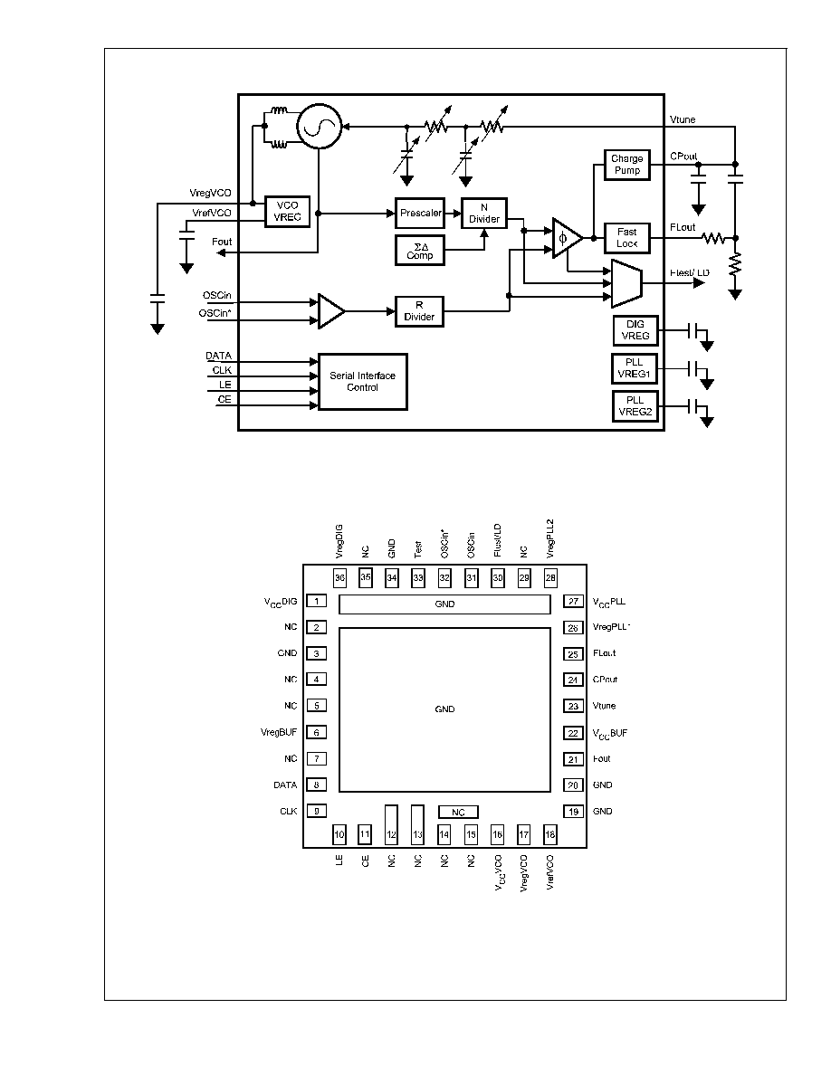
Functional Block Diagram
20101101
Connection Diagram
36-Pin LLP (LQ) Package
20101102
LMX2531
www.national.com
2
Pin Descriptions
Pin
Number
Pin Name
I/O Description
1
VccDIG
-
Power Supply for digital LDO circuitry. Input may range from 2.8 - 3.2 V. Bypass capacitors should be
placed as close as possible to this pin and ground.
3
GND
-
Ground
2,4,5,7,
12,
13,
29, 35
NC
-
No Connect.
6
VregBUF
-
Internally regulated voltage for the VCO buffer circuitry. Connect to ground with a capacitor.
8
DATA
I
MICROWIRE serial data input. High impedance CMOS input. This pin must not exceed 2.75V. Data is
clocked in MSB first. The last bits clocked in form the control or register select bits.
9
CLK
I
MICROWIRE clock input. High impedance CMOS input. This pin must not exceed 2.75V. Data is
clocked into the shift register on the rising edge.
10
LE
I
MICROWIRE Latch Enable input. High impedance CMOS input. This pin must not exceed 2.75V.
Data stored in the shift register is loaded into the selected latch register when LE goes HIGH.
11
CE
I
Chip Enable Input. High impedance CMOS input. This pin must not exceed 2.75V. When CE is
brought high the LMX2531 is powered up corresponding to the internal power control bits. It is
necessary to reprogram the R0 register to get the part to re-lock.
14, 15
NC
-
No Connect. Do NOT ground.
16
VccVCO
-
Power Supply for VCO regulator circuitry. Input may range from 2.8 - 3.2 V. Bypass capacitors should
be placed as close as possible to this pin and ground.
17
VregVCO
-
Internally regulated voltage for VCO circuitry. Not intended to drive an external load. Connect to
ground with a capacitor and some series resistance.
18
VrefVCO
-
Internal reference voltage for VCO LDO. Not intended to drive an external load. Connect to ground
with a capacitor.
19
GND
-
Ground for the VCO circuitry.
20
GND
-
Ground for the RF Output Buffer circuitry.
21
Fout
O Buffered RF Output for the VCO.
22
VccBUF
-
Power Supply for the VCO Buffer circuitry. Input may range from 2.8 - 3.2 V. Bypass capacitors
should be placed as close as possible to this pin and ground.
23
Vtune
I
Tuning voltage input for the VCO. For connection to the CPout Pin through an external passive loop
filter.
24
CPout
O Charge pump output for PLL. For connection to Vtune through an external passive loop filter.
25
FLout
O An open drain NMOS output which is used for FastLock or a general purpose output.
26
VregPLL1
-
Internally regulated voltage for PLL charge pump. Not intended to drive an external load. Connect to
ground with a capacitor.
27
VccPLL
-
Power Supply for the PLL. Input may range from 2.8 - 3.2 V. Bypass capacitors should be placed as
close as possible to this pin and ground.
28
VregPLL2
-
Internally regulated voltage for RF digital circuitry. Not intended to drive an external load. Connect to
ground with a capacitor.
30
Ftest/LD
O Multiplexed CMOS output. Typically used to monitor PLL lock condition.
31
OSCin
I
Oscillator input. The oscillator can be placed in either single-ended or differential mode of operation.
32
OSCin*
I
Oscillator complimentary input. When a single ended source is used, then a bypass capacitor should
be placed as close as possible to this pin and be connected to ground.
33
Test
O This pin if for test purposes and should be grounded for normal operation.
34
GND
-
Ground
36
VregDIG
-
Internally regulated voltage for LDO digital circuitry.
LMX2531
www.national.com
3
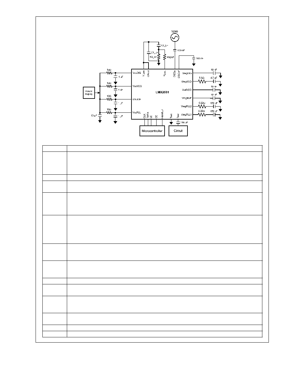
Connection Diagram
20101111
Pin(s)
Application Information
VccDIG
VccVCO
VccBUF
VccPLL
Because the LMX2531 contains internal regulators, the power supply noise rejection is very good and
capacitors at this pin are not critical. If desired, capacitors can be placed at these pins to improve the noise
rejection. Recommended values are from open to 1 µF.
VregDIG
There is not really any reason to use any other values than the recommended values.
VrefVCO
If the VregVCO capacitor is changed, it is recommended to keep this capacitor between 1/100 and 1/1000 of
the value of the VregVCO capacitor.
VregVCO
Because this pin is the output of a regulator, there are be stability concerns if there is not sufficient series
resistance. For ceramic capacitors the ESR (Equivalent Series Resistance) is too low, and it recommended
that a series resistance of 1 - 3.3
is necessary. If there is insufficient ESR, then there may be degradation in
the phase noise, especially in the 100 - 300 kHz offset. Recommended values are from 1 µF to 10 µF.
VregPLL1
VregPLL2
The choice of the capacitor value at this pin involves a trade-off between integer spurs and phase noise in the
100 - 300 kHz offset range. If too much series resistance is at this pin, the spurs at far offset will be severely
degraded. If there is too little, the phase noise may be degraded. A 470 nF capacitor in series with 220 m
provides optimal spurs with a minimal degradation in phase noise, although these optimal values may be
design specific.
CLK
DATA
LE
Since the maximum voltage on these pins is less than the minimum Vcc voltage, level shifting may be
required, if the output voltage of the microcontroller is too high. This can be accomplished with a resistive
divider.
CE
As with the CLK, DATA, and LE pins, level shifting may be required if the output voltage of the microcontroller
is too high. A resistive divider is or a series diode are two ways to accomplish this. The diode has the
advantage that no current flows through it when the chip is powered down.
Ftest/LD
It is an option to use the lock detect information from this pin.
Fout
This is the high frequency output. This needs to be AC coupled, and matching may also be required. The
value of the DC blocking capacitor may be changed, depending on the output frequency.
CPout
Vtune
In most cases, it is sufficient to short these together. C1_LF, C2_LF, and R2_LF are used in conjunction with
the internal loop filter to make a fourth order loop filter. However, the user always has the option of adding
additional poles.
R2pLF
This is the fastlock resistor, which can be useful in many cases, since the spurs are often better with low
charge pump currents, and the internal loop filter can be adjusted during fastlock.
OSCin
This is the crystal oscillator input pin. It needs to be AC coupled.
OSCin*
If the device is being driven single-ended, this pin needs to be shunted to ground with a capacitor.
LMX2531
www.national.com
4
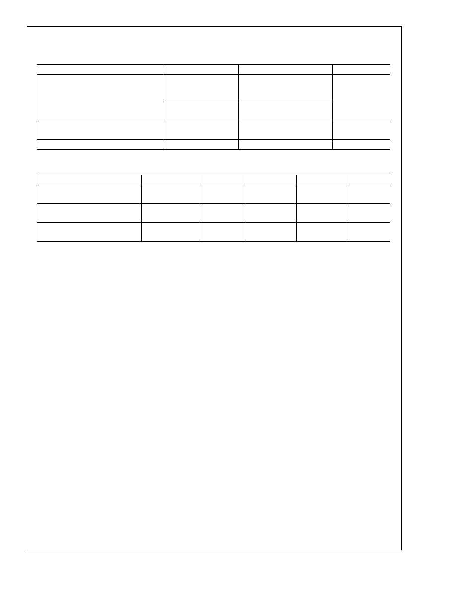
Absolute Maximum Ratings
(Note 1)
If Military/Aerospace specified devices are required, please contact the National Semiconductor Sales Office/
Distributors for availability and specifications.
Parameter
Symbol
Ratings
Units
Power Supply Voltage
V
CC
(VccDIG, VccVCO,
VccBUF, VccPLL)
-0.3 to 3.5
V
All other pins (Except
Ground)
-0.3 to 3.0
Storage Temperature
Range
T
STG
-65 to 150
∞C
Lead Temperature (solder 4 sec.)
T
L
+ 260
∞C
Recommended Operating Conditions
Parameter
Symbol
Min
Typ
Max
Units
Power Supply Voltage
(VccDig, VccVCO, VccBUF)
Vcc
2.8
3.0
3.2
V
Serial Interface and Power Control
Voltage
V
i
0
2.75
V
Ambient Temperature
(Note 3)
T
A
-40
+85
∞C
Note 1: Absolute Maximum Ratings indicate limits beyond which damage to the device may occur. Recommended Operating Conditions indicate conditions for
which the device is intended to be functional, but do not guarantee specific performance limits. For guaranteed specifications and test conditions, see the Electrical
Characteristics. The guaranteed specifications apply only to the test conditions listed.
LMX2531
www.national.com
5