LP2985LV
Micropower 150 mA Low-Noise Low-Dropout Regulator
in SOT-23 and micro SMD packages for Applications
with Output Voltages
2.3V
Designed for Use with Very Low ESR Output Capacitors
General Description
The LP2985LV is a 150 mA, fixed-output voltage regulator
designed to providehigh performance and low noise in ap-
plications requiring output voltages
<
2.3V.
Using an optimized VIP
TM
(Vertically Integrated PNP) pro-
cess, the LP2985LV delivers unequalled performance in all
specifications critical to battery-powered designs:
Ground Pin Current: Typically 825 µA
@
150 mA load, and
75 µA
@
1 mA load.
Enhanced Stability: The LP2985LV is stable with output
capacitor ESR as low as 5 m
, which allows the use of
ceramic capacitors on the output.
Sleep Mode: Less than 1 µA quiescent current when ON/
OFF pin is pulled low.
Smallest Possible Size: micro SMD package uses absolute
minimum board space.
Precision Output: 1% tolerance output voltages available
(A grade).
Low Noise: By adding a 10 nF bypass capacitor, output
noise can be reduced to 30 µV (typical).
Features
n
Guaranteed 150 mA output current
n
Smallest possible size (micro SMD)
n
Requires minimum external components
n
Stable with low-ESR output capacitor
n
<
1 µA quiescent current when shut down
n
Low ground pin current at all loads
n
Output voltage accuracy 1% (A Grade)
n
High peak current capability
n
Wide supply voltage range (16V max)
n
Low Z
OUT
: 0.3
typical (10 Hz to 1 MHz)
n
Overtemperature/overcurrent protection
n
-40∞C to +125∞C junction temperature range
n
Custom voltages available
Applications
n
Cellular Phone
n
Palmtop/Laptop Computer
n
Personal Digital Assistant (PDA)
n
Camcorder, Personal Stereo, Camera
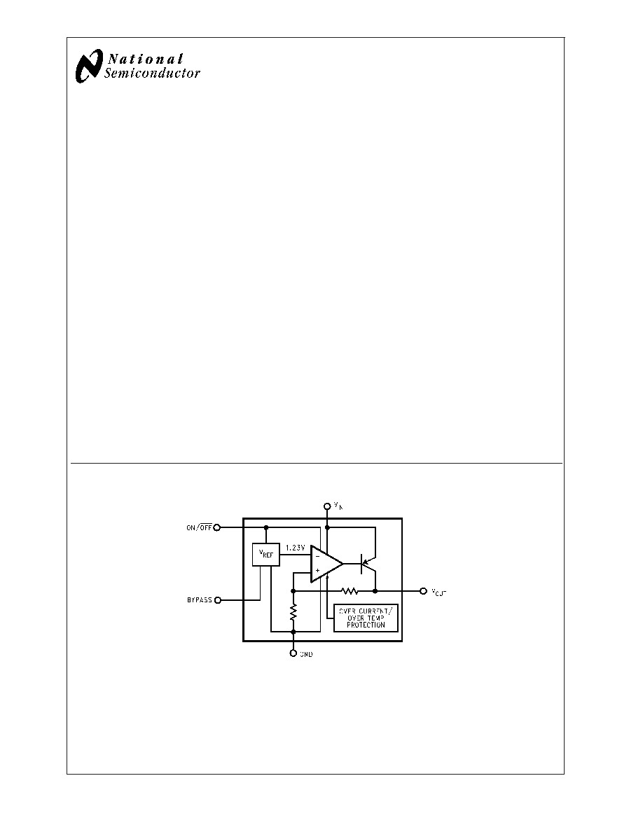
Block Diagram
10129501
VIP
TM
is a trademark of National Semiconductor Corporation.
May 2004
LP2985L
V
Micropower
150
mA
Low-Noise
Low-Dropout
Regulator
in
SOT
-23
and
micro
SMD
packages
for
Applications
with
Output
V
oltages
2.3V
© 2004 National Semiconductor Corporation
DS101295
www.national.com
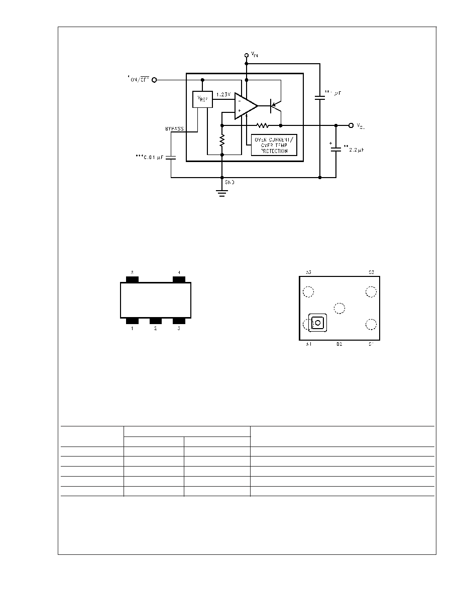
Basic Application Circuit
10129502
*ON/OFF input must be actively terminated. Tie to V
IN
if this function is not to be used.
**Minimum capacitance is shown to ensure stability (may be increased without limit). Ceramic capacitor required for output (see Application Hints).
***Reduces output noise (may be omitted if application is not noise critical). Use ceramic or film type with very low leakage current (see Application Hints).
Connection Diagrams
5-Lead Small Outline Package (M5)
micro SMD, 5 Bump Package (BPA05 & BLA05)
10129503
Top View
See NS Package Number MF05A
For ordering information see Table 1
10129523
Note: The actual physical placement of the package marking will vary from
part to part. Package marking contains date code and lot traceability
information, and will vary considerably. Package marking does not correlate
to device type.
Top View
See NS Package Number BPA05 & BLA05
Pin Descrption
Name
Pin Number
Function
SOT-23
micro SMD
V
IN
1
C3
Input Voltage
GND
2
A1
Common Ground (device substrate)
ON/OFF
3
A3
Logic high enable input
BYPASS
4
B2
Bypass capacitor for low noise operation
V
OUT
5
C1
Regulated output voltage
LP2985L
V
www.national.com
2
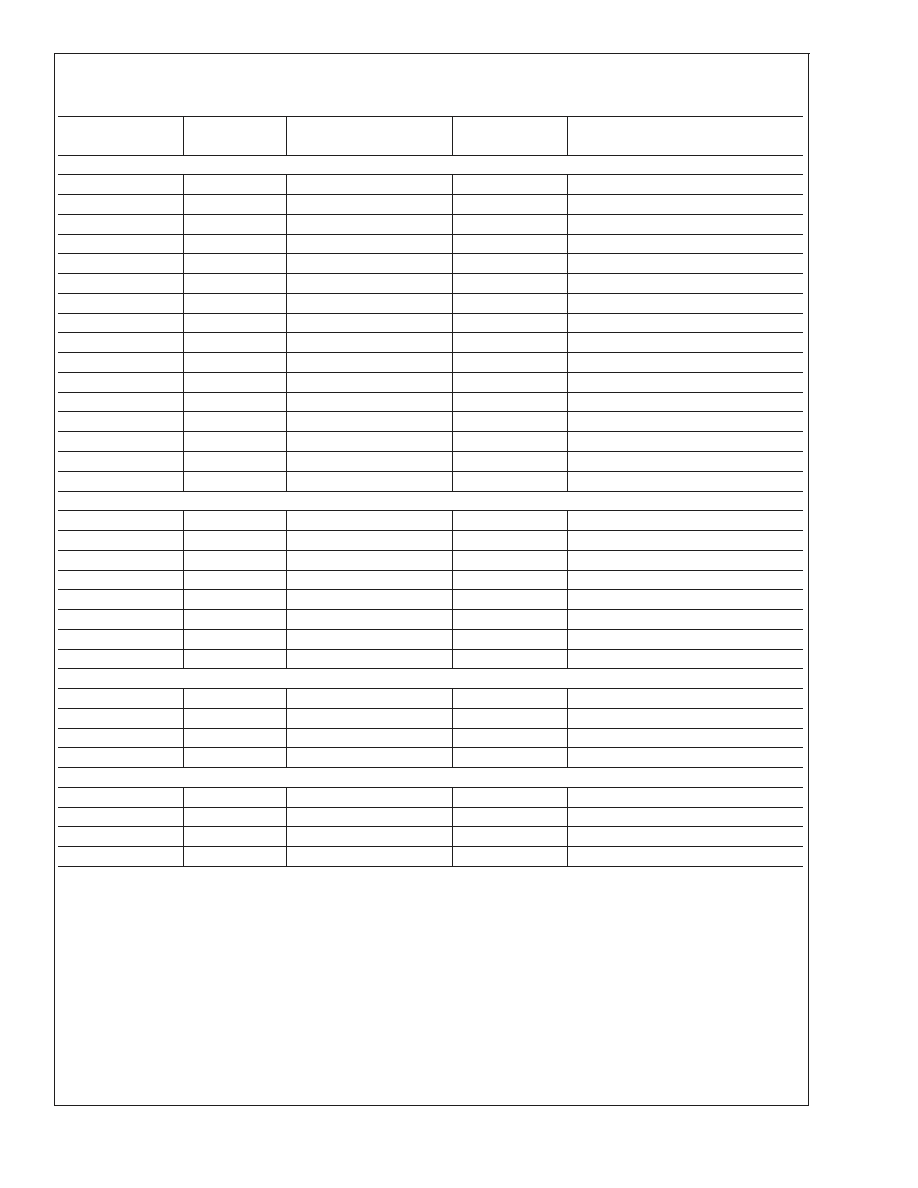
Ordering Information
TABLE 1. Package Marking and Ordering Information
Output Voltage (V)
Grade
Order Information
Package
Marking
Supplied as:
5-Lead Small Outline Package (M5)
1.35
A
LP2985AIM5X-135
LF7A
3000 Units on Tape and Reel
1.35
A
LP2985AIM5-135
LF7A
1000 Units on Tape and Reel
1.35
STD
LP2985IM5X-135
LF7B
3000 Units on Tape and Reel
1.35
STD
LP2985IM5-135
LF7B
1000 Units on Tape and Reel
1.5
A
LP2985AIM5X-1.5
LCHA
3000 Units on Tape and Reel
1.5
A
LP2985AIM5-1.5
LCHA
1000 Units on Tape and Reel
1.5
STD
LP2985IM5X-1.5
LCHB
3000 Units on Tape and Reel
1.5
STD
LP2985IM5-1.5
LCHB
1000 Units on Tape and Reel
1.8
A
LP2985AIM5X-1.8
LAYA
3000 Units on Tape and Reel
1.8
A
LP2985AIM5-1.8
LAYA
1000 Units on Tape and Reel
1.8
STD
LP2985IM5X-1.8
LAYB
3000 Units on Tape and Reel
1.8
STD
LP2985IM5-1.8
LAYB
1000 Units on Tape and Reel
2.0
A
LP2985AIM5X-2.0
LCDA
3000 Units on Tape and Reel
2.0
A
LP2985AIM5-2.0
LCDA
1000 Units on Tape and Reel
2.0
STD
LP2985IM5X-2.0
LCDB
3000 Units on Tape and Reel
2.0
STD
LP2985IM5-2.0
LCDB
1000 Units on Tape and Reel
micro SMD, 5 Bump Package (BPA05 - 170 µm ball)
1.5
A
LP2985AIBP-1.5
250 Units on Tape and Reel
1.5
A
LP2985AIBPX-1.5
3000 Units on Tape and Reel
1.5
STD
LP2985IBP-1.5
250 Units on Tape and Reel
1.5
STD
LP2985IBPX-1.5
3000 Units on Tape and Reel
1.8
A
LP2985AIBP-1.8
250 Units on Tape and Reel
1.8
A
LP2985AIBPX-1.8
3000 Units on Tape and Reel
1.8
STD
LP2985IBP-1.8
250 Units on Tape and Reel
1.8
STD
LP2985IBPX-1.8
3000 Units on Tape and Reel
micro SMD, 5 Bump Package (BLA05 - 300 µm ball)
1.8
A
LP2985AIBL-1.8
250 Units on Tape and Reel
1.8
A
LP2985AIBLX-1.8
3000 Units on Tape and Reel
1.8
STD
LP2985IBL-1.8
250 Units on Tape and Reel
1.8
STD
LP2985IBLX-1.8
3000 Units on Tape and Reel
micro SMD, 5 Bump Package (TPA05 - 170 µm ball)
1.8
A
LP2985AITP-1.8
250 Units on Tape and Reel
1.8
A
LP2985AITPX-1.8
3000 Units on Tape and Reel
1.8
STD
LP2985ITP-1.8
250 Units on Tape and Reel
1.8
STD
LP2985ITPX-1.8
3000 Units on Tape and Reel
LP2985L
V
www.national.com
3
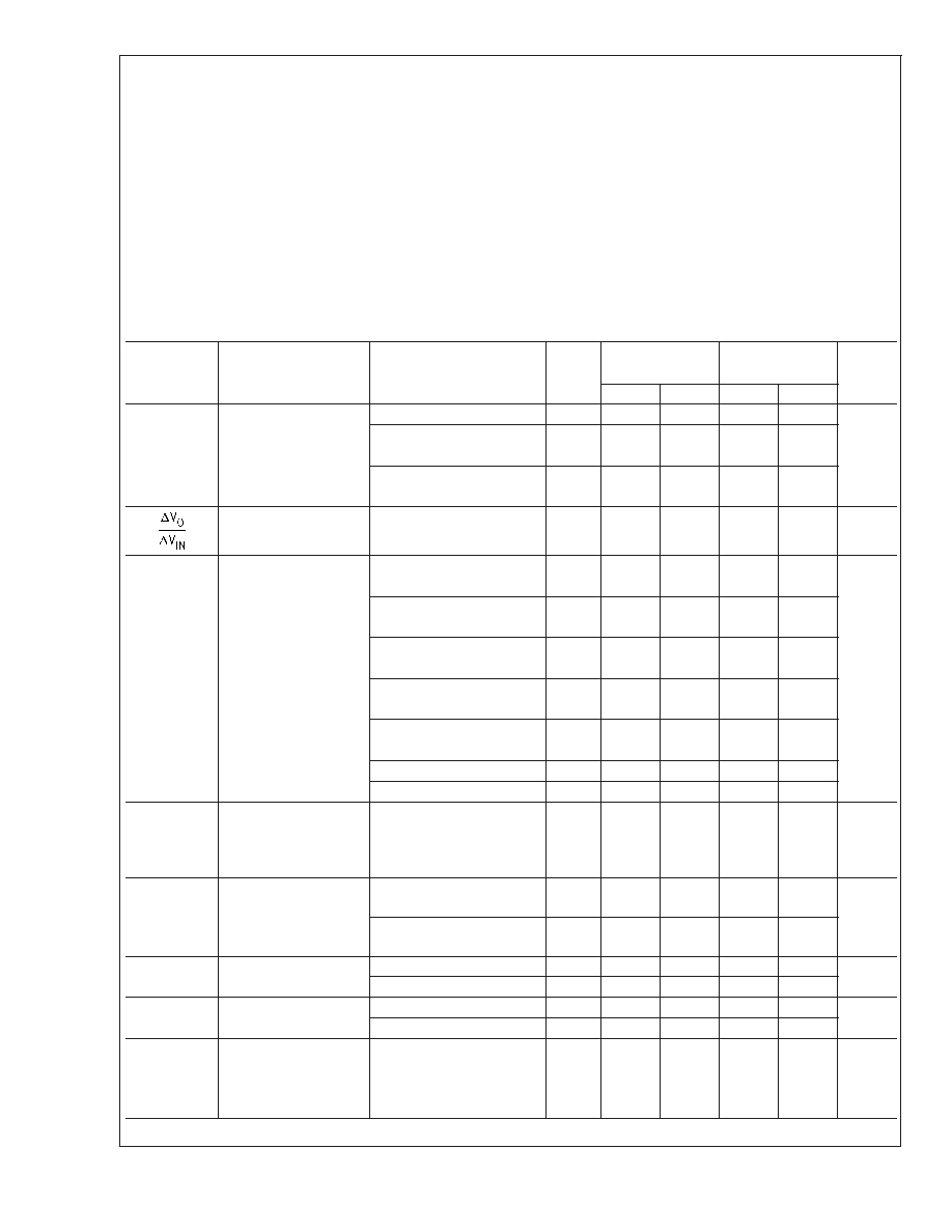
Absolute Maximum Ratings
(Note 1)
If Military/Aerospace specified devices are required,
please contact the National Semiconductor Sales Office/
Distributors for availability and specifications.
Storage Temperature Range
-65∞C to +150∞C
Operating Junction Temperature
Range
-40∞C to +125∞C
Lead Temp. (Soldering, 5 sec.)
260∞C
ESD Rating (Note 2)
2 kV
Power Dissipation (Note 3)
Internally Limited
Input Supply Voltage (Survival)
-0.3V to +16V
Input Supply Voltage (Operating)
2.2V to +16V
Shutdown Input Voltage (Survival)
-0.3V to +16V
Output Voltage (Survival, (Note 4))
-0.3V to +9V
I
OUT
(Survival)
Short Circuit
Protected
Input-Output Voltage (Survival,
-0.3V to +16V
(Note 5))
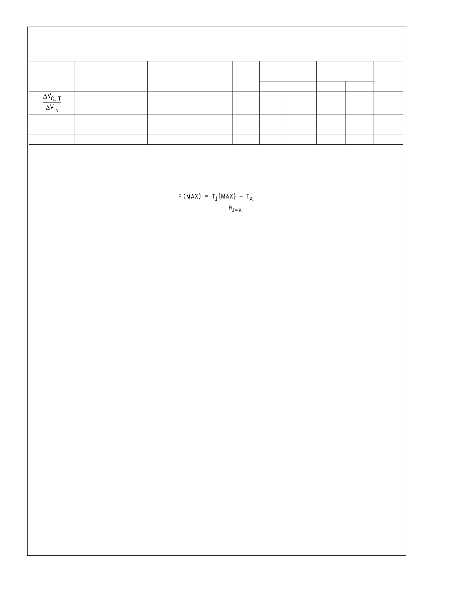
Electrical Characteristics
(Note 10)
Limits in standard typeface are for T
J
= 25∞C. and limits in boldface type apply over the full operating temperature range. Un-
less otherwise specified: V
IN
= V
O
(NOM) + 1V, I
L
= 1 mA, C
IN
= 1 µF, C
OUT
= 4.7 µF, V
ON/OFF
= 2V.
Symbol
Parameter
Conditions
Typ
LP2985AI-X.X
LP2985I-X.X
Units
(Note 6)
(Note 6)
Min
Max
Min
Max
V
O
Output Voltage
Tolerance
I
L
= 1 mA
-1.0
1.0
-1.5
1.5
%V
NOM
1 mA
I
L
50 mA
-1.5
1.5
-2.5
2.5
-2.5
2.5
-3.5
3.5
1 mA
I
L
150 mA
-2.5
2.5
-3.0
3.0
-3.5
3.5
-4.0
4.0
Output Voltage
V
O
(NOM)+1V
V
IN
16V
0.007
0.014
0.014
%/V
Line Regulation
0.032
0.032
I
GND
Ground Pin Current
I
L
= 0
65
95
95
µA
125
125
I
L
= 1 mA
75
110
110
170
170
I
L
= 10 mA
120
220
220
400
400
I
L
= 50 mA
300
500
500
900
900
I
L
= 150 mA
825
1200
1200
2000
2000
V
ON/OFF
<
0.3V
0.01
0.8
0.8
V
ON/OFF
<
0.15V
0.05
2
2
V
IN
(min)
Minimum Input Voltage
Required To maintain
Output Regulation
(Note 9)
2.05
2.20
2.20
V
V
IN
- V
OUT
Dropout Voltage
(Note 9)
IL = 50mA
120
150
250
150
250
mV
IL = 150mA
280
350
600
350
600
V
ON/OFF
ON/OFF Input Voltage
(Note 7)
High = O/P ON
1.4
1.6
1.6
V
Low = O/P OFF
0.55
0.15
0.15
I
ON/OFF
ON/OFF Input Current
V
ON/OFF
= 0
0.01
-2
-2
µA
V
ON/OFF
= 5V
5
15
15
e
n
Output Noise
BW = 300 Hz to 50 kHz,
Voltage (RMS)
C
OUT
= 10 µF
30
µV
C
BYPASS
= 10 nF
V
OUT
= 1.8V
LP2985L
V
www.national.com
4
Electrical Characteristics
(Note 10) (Continued)
Limits in standard typeface are for T
J
= 25∞C. and limits in boldface type apply over the full operating temperature range. Un-
less otherwise specified: V
IN
= V
O
(NOM) + 1V, I
L
= 1 mA, C
IN
= 1 µF, C
OUT
= 4.7 µF, V
ON/OFF
= 2V.
Symbol
Parameter
Conditions
Typ
LP2985AI-X.X
LP2985I-X.X
Units
(Note 6)
(Note 6)
Min
Max
Min
Max
Ripple Rejection
f = 1 kHz, C
BYPASS
= 10 nF
45
dB
C
OUT
= 10 µF
I
O
(SC)
Short Circuit Current
R
L
= 0 (Steady State)
400
mA
(Note 8)
I
O
(PK)
Peak Output Current
V
OUT
V
o
(NOM) -5%
350
mA
Note 1: "Absolute Maximum Ratings" indicate limits beyond which damage to the component may occur. Electrical specifications do not apply when operating the
device outside of its rated operating conditions.
Note 2: The ESD rating of pins 3 and 4 for the SOT-23 package, or pins 5 and 2 for the micro SMD package, is 1 kV.
Note 3: The maximum allowable power dissipation is a function of the maximum junction temperature, T
J
(MAX), the junction-to-ambient thermal resistance,
J-A
,
and the ambient temperature, T
A
. The maximum allowable power dissipation at any ambient temperture is calculated using:
Where the value of
J-A
for the SOT-23 package is 220∞C/W in a typical PC board mounting. Exceeding the maximum allowable dissipation will cause excessive die
temperature, and the regulator will go into thermal shutdown.
Note 4: If used in a dual-supply system where the regulator load is returned to a negative supply, the LP2985LV output must be diode-clamped to ground.
Note 5: The output PNP structure contains a diode between the V
IN
to V
OUT
terminals that is normally reverse-biased. Reversing the polarity from V
IN
to V
OUT
will
turn on this diode, and possibly damage the device (See Application Hints).
Note 6: Limits are 100% production tested at 25∞C. Limits over the operating temperature range are guaranteed through correlation using Statistical Quality Control
(SQC) methods. The limits are used to calculate National's Average Outgoing Quality Level (AOQL).
Note 7: The ON/OFF input must be properly driven to prevent possible misoperation. For details, refer to Application Hints.
Note 8: The LP2985LV has foldback current limiting which allows a high peak current when V
OUT
>
0.5V, and then reduces the maximum output current as V
OUT
is forced to ground (see Typical Performance Characteristics curves).
Note 9: V
IN
must be the greater of 2.2V or V
OUT(nom)
+ Dropout Voltage to maintain output regulation. Dropout Voltage is defined as the input to output differential
at which the output voltage drops 2% below ther value measured with a 1V differential.
Note 10: Exposing the micro SMD device to direct sunlight will cause misoperation. See Application Hints for additional information.
LP2985L
V
www.national.com
5