LP3891
0.8A Fast-Response Ultra Low Dropout Linear
Regulators
General Description
The LP3891 is a high current, fast response regulator which
can maintain output voltage regulation with minimum input to
output voltage drop. Fabricated on a CMOS process, the
device operates from two input voltages: Vbias provides
voltage to drive the gate of the N-MOS power transistor,
while Vin is the input voltage which supplies power to the
load. The use of an external bias rail allows the part to
operate from ultra low Vin voltages. Unlike bipolar regula-
tors, the CMOS architectutre consumes extremely low qui-
escent current at any output load current. The use of an
N-MOS power transistor results in wide bandwidth, yet mini-
mum external capacitance is required to maintain loop sta-
bility.
The fast transient response of these devices makes them
suitable for use in powering DSP, Microcontroller Core volt-
ages and Switch Mode Power Supply post regulators. The
parts are available in TO-220 and TO-263 packages.
Dropout Voltage: 100 mV (typ)
@
0.8A load current.
Ground Pin Current: 3 mA (typ) at full load.
Shutdown Current: 60 nA (typ) when S/D pin is low.
Precision Output Voltage: 1.5% room temperature accu-
racy.
Features
n
Ultra low dropout voltage (100mV
@
0.8A typ)
n
Low ground pin current
n
Load regulation of 0.04%/A
n
60 nA typical quiescent current in shutdown
n
1.5% output accuracy (25∞C)
n
TO-220, TO-263 packages
n
Over temperature/over current protection
n
-40∞C to +125∞C junction temperature range
Applications
n
DSP Power Supplies
n
Server Core and I/O Supplies
n
PC Add-in-Cards
n
Local Regulators in Set-Top Boxes
n
Microcontroller Power Supplies
n
High Efficiency Power Supplies
n
SMPS Post-Regulators
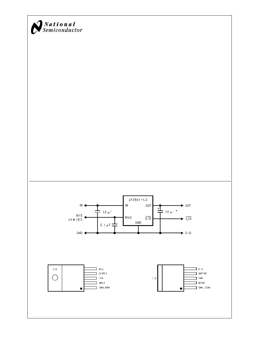
Typical Application Circuit
20069501
At least 10 µF of input and output capacitance is required for stability.
*Tantalum capacitors are recommended. Aluminum electrolytic capacitors may be used for restricted temperature range. See application hints.
Connection Diagrams
20069502
TO-220, Top View
20069503
TO-263, Top View
September 2003
LP3891
0.8A
Fast-Response
Ultra
Low
Dropout
Linear
Regulators
© 2003 National Semiconductor Corporation
DS200695
www.national.com
Ordering Information
Order Number
Package Type
Package Drawing
Supplied As
LP3891ES-1.2
TO263-5
TS5B
Rail
LP3891ESX-1.2
TO263-5
TS5B
Tape and Reel
LP3891ET-1.2
TO220-5
T05D
Rail
LP3891ES-1.5
TO263-5
TS5B
Rail
LP3891ESX-1.5
TO263-5
TS5B
Tape and Reel
LP3891ET-1.5
TO220-5
T05D
Rail
LP3891ES-1.8
TO263-5
TS5B
Rail
LP3891ESX-1.8
TO263-5
TS5B
Tape and Reel
LP3891ET-1.8
TO220-5
T05D
Rail
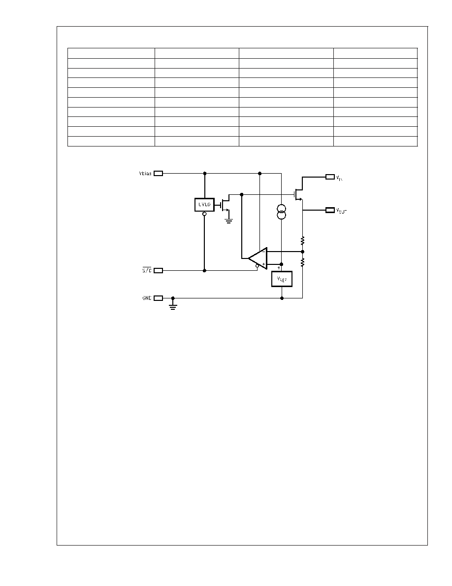
Block Diagram
20069524
LP3891
www.national.com
2
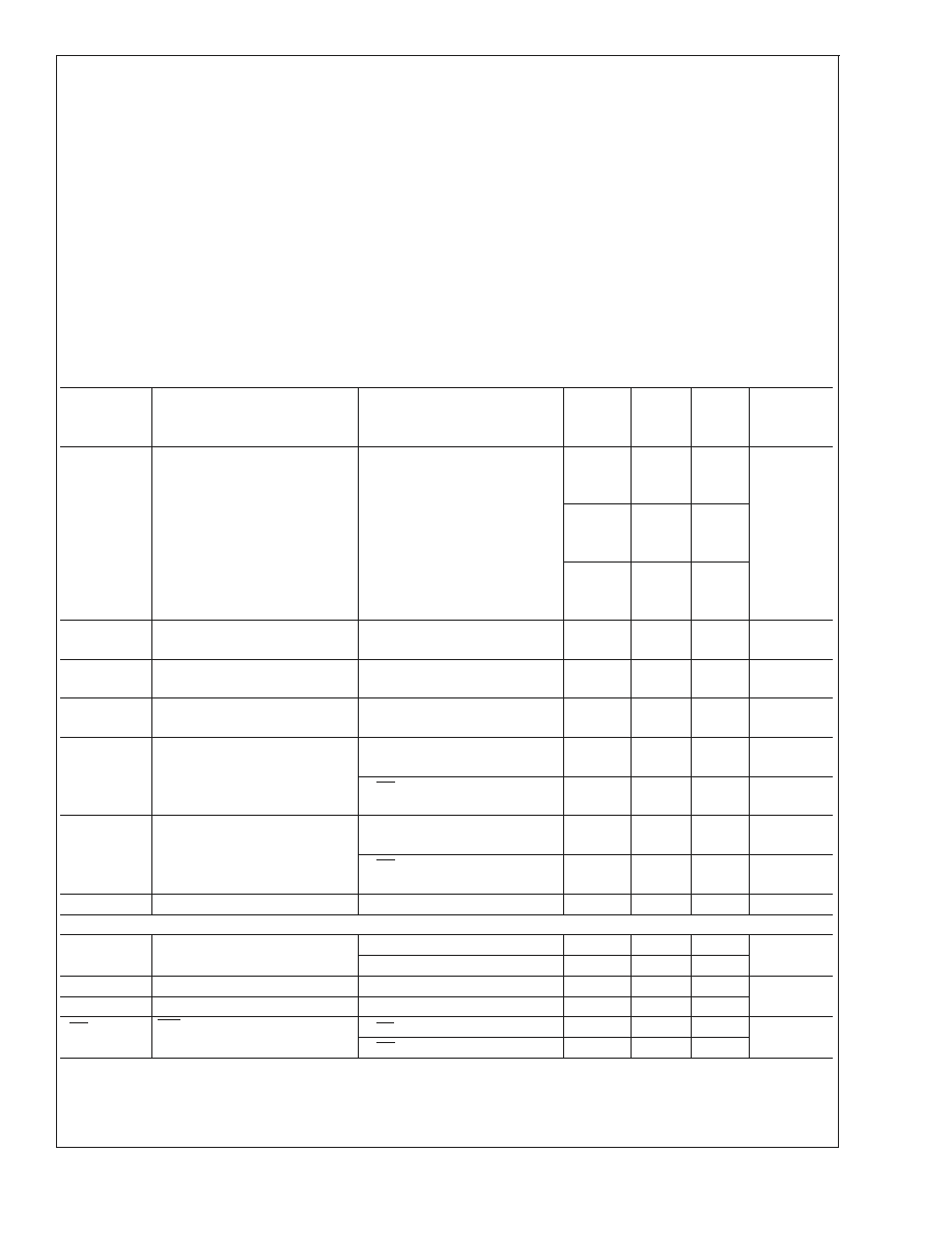
Absolute Maximum Ratings
(Note 1)
If Military/Aerospace specified devices are required,
please contact the National Semiconductor Sales Office/
Distributors for availability and specifications.
Storage Temperature Range
-65∞C to +150∞C
Lead Temp. (Soldering, 5 seconds)
260∞C
ESD Rating
Human Body Model (Note 3)
Machine Model (Note 10)
2 kV
200V
Power Dissipation (Note 2)
Internally Limited
V
IN
Supply Voltage (Survival)
-0.3V to +6V
V
BIAS
Supply Voltage (Survival)
-0.3V to +7V
Shutdown Input Voltage (Survival)
-0.3V to +7V
I
OUT
(Survival)
Internally Limited
Output Voltage (Survival)
-0.3V to +6V
Junction Temperature
-40∞C to +150∞C
Operating Ratings
V
IN
(V
OUT
+ V
DO
) to 5.5V
Shutdown
0 to +6V
I
OUT
0.8A
Junction Temperature
-40∞C to +125∞C
V
BIAS
4.5V to 6V
Electrical Characteristics
Limits in standard typeface are for T
J
= 25∞C, and limits in boldface type apply
over the full operating temperature range. Unless otherwise specified: V
IN
= V
O
(NOM) + 1V, V
BIAS
= 4.5V, I
L
= 10 mA, C
IN
=
C
OUT
= 10 µF, V
S/D
= V
BIAS
.
Symbol
Parameter
Conditions
Typical
(Note 4)
MIN
(Note
5)
MAX
(Note
5)
Units
V
O
Output Voltage Tolerance
10 mA
I
L
0.8A
V
O
(NOM) + 1V
V
IN
5.5V
4.5V
V
BIAS
6V
1.216
1.198
1.186
1.234
1.246
V
1.5
1.478
1.455
1.522
1.545
1.8
1.773
1.746
1.827
1.854
V
O
/
V
IN
Output Voltage Line Regulation
(Note 7)
V
O
(NOM) + 1V
V
IN
5.5V
0.01
%/V
V
O
/
I
L
Output Voltage Load Regulation
(Note 8)
10 mA
I
L
0.8A
0.04
0.06
%/A
V
DO
Dropout Voltage (Note 9)
I
L
= 0.8A
100
300
400
mV
I
Q
(V
IN
)
Quiescent Current Drawn from
V
IN
Supply
10 mA
I
L
0.8A
3
7
8
mA
V
S/D
0.3V
0.03
1
30
µA
I
Q
(V
BIAS
)
Quiescent Current Drawn from
V
BIAS
Supply
10 mA
L
0.8A
1
2
3
mA
V
S/D
0.3V
0.03
1
30
µA
I
SC
Short-Circuit Current
V
OUT
= 0V
1.8
A
Shutdown Input
V
SDT
Output Turn-off Threshold
Output = ON
0.7
1.3
V
Output = OFF
0.7
0.3
Td (OFF)
Turn-OFF Delay
R
LOAD
X C
OUT
<<
Td (OFF)
20
µs
Td (ON)
Turn-ON Delay
R
LOAD
X C
OUT
<<
Td (ON)
15
I
S/D
S/D Input Current
V
S/D
=1.3V
1
µA
V
S/D
0.3V
-1
LP3891
www.national.com
3
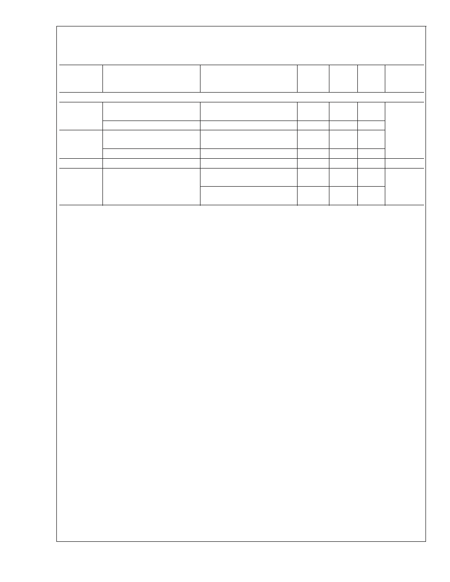
Electrical Characteristics
Limits in standard typeface are for T
J
= 25∞C, and limits in boldface type apply
over the full operating temperature range. Unless otherwise specified: V
IN
= V
O
(NOM) + 1V, V
BIAS
= 4.5V, I
L
= 10 mA, C
IN
=
C
OUT
= 10 µF, V
S/D
= V
BIAS
. (Continued)
Symbol
Parameter
Conditions
Typical
(Note 4)
MIN
(Note
5)
MAX
(Note
5)
Units
AC Parameters
PSRR (V
IN
)
Ripple Rejection for V
IN
Input
Voltage
V
IN
= V
OUT
+1V, f = 120 Hz
80
dB
V
IN
= V
OUT
+ 1V, f = 1 kHz
65
PSRR
(V
BIAS
)
Ripple Rejection for V
BIAS
Voltage
V
BIAS
= V
OUT
+ 3V, f = 120 Hz
70
V
BIAS
= V
OUT
+ 3V, f = 1 kHz
65
Output Noise Density
f = 120 Hz
1
µV/root-Hz
e
n
Output Noise Voltage
BW = 10 Hz - 100 kHz, V
OUT
=
1.8V
150
µV (rms)
BW = 300 Hz - 300 kHz, V
OUT
= 1.8V
90
Note 1: Absolute maximum ratings indicate limits beyond which damage to the component may occur. Operating ratings indicate conditions for which the device
is intended to be functional, but do not guarantee specific performance limits. For guaranteed specifications, see Electrical Characteristics. Specifications do not
apply when operating the device outside of its rated operating conditions.
Note 2: At elevated temperatures, device power dissipation must be derated based on package thermal resistance and heatsink thermal values.
J-A
for TO-220
devices is 65∞C/W if no heatsink is used. If the TO-220 device is attached to a heatsink, a
J-S
value of 4∞C/W can be assumed.
J-A
for TO-263 devices is
approximately 40∞C/W if soldered down to a copper plane which is at least 1.5 square inches in area. If power dissipation causes the junction temperature to exceed
specified limits, the device will go into thermal shutdown.
Note 3: The human body model is a 100 pF capacitor discharged through a 1.5k resistor into each pin.
Note 4: Typical numbers represent the most likely parametric norm for 25∞C operation.
Note 5: Limits are guaranteed through testing, statistical correlation, or design.
Note 6: If used in a dual-supply system where the regulator load is returned to a negative supply, the output pin must be diode clamped to ground.
Note 7: Output voltage line regulation is defined as the change in output voltage from nominal value resulting from a change in input voltage.
Note 8: Output voltage load regulation is defined as the change in output voltage from nominal value as the load current increases from no load to full load.
Note 9: Dropout voltage is defined as the minimum input to output differential required to maintain the output with 2% of nominal value.
Note 10: The machine model is a 220 pF capacitor discharged directly into each pin. The machine model ESD rating of pin 5 is 100V.
LP3891
www.national.com
4
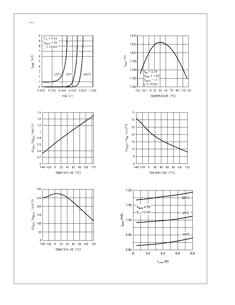
Typical Performance Characteristics
Unless otherwise specified: T
J
= 25∞C, C
OUT
= 10 µF, Cin =
10µF, S/D pin is tied to V
BIAS
, V
IN
= 2.2V, V
OUT
= 1.8V
I
GND
vs VSD
V
OUT
vs Temperature
20069505
20069506
DC Load Regulation
Line Regulation vs V
IN
20069507
20069508
Line Regulation vs V
BIAS
I
BIAS
vs I
L
20069509
20069510
LP3891
www.national.com
5