LP3990
150mA Linear Voltage Regulator for Digital Applications
General Description
The LP3990 regulator is designed to meet the requirements
of portable, battery-powered systems providing an accurate
output voltage, low noise, and low quiescent current. The
LP3990 will provide a 0.8V output from the low input voltage
of 2V at up to 150mA load current. When switched into
shutdown mode via a logic signal at the enable pin, the
power consumption is reduced to virtually zero.
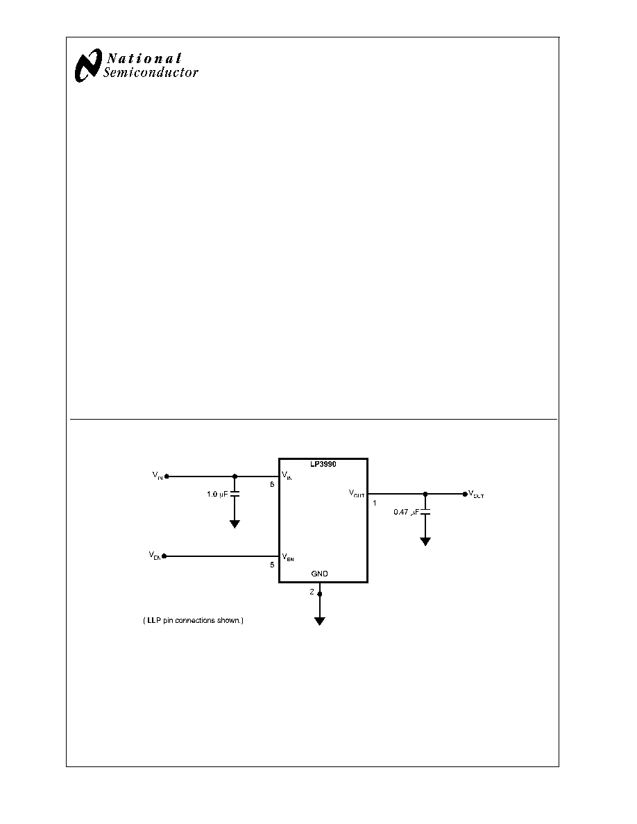
The LP3990 is designed to be stable with space saving
ceramic capacitors as small as 0.47µF.
Performance is specified for a -40∞C to 125∞C junction tem-
perature range.
For output voltages other than 0.8V, 1.35V, 1.5V, 1.8V, 2.5V,
2.8V, or 3.3V please contact your local NSC sales office.
Features
n
1% Voltage Accuracy at Room Temperature
n
Stable with Ceramic Capacitor
n
Logic Controlled Enable
n
No Noise Bypass Capacitor Required
n
Thermal-Overload and Short-Circuit Protection
Key Specifications
n
Input Voltage Range
2.0 to 6.0V
n
Output Voltage Range
0.8 to 3.3V
n
Output Current
150mA
n
Output Stable - Capacitors
0.47uF
n
Virtually Zero I
Q
(Disabled)
<
10nA
n
Very Low I
Q
(Enabled)
43uA
n
Low Output Noise
150uV
RMS
n
PSRR
55dB at 1kHz
n
Fast Start Up
105us
Package
All available in Lead Free option.
4 Pin micro SMD
1 mm x 1.28mm
6 pin LLP (SOT23 footprint)
SOT23 - 5
For other package options contact your NSC sales office.
Applications
n
Cellular Handsets
n
Hand-Held Information Appliances
Typical Application Circuit
20076801
November 2004
LP3990
150mA
Linear
V
oltage
Regulator
for
Digital
Applications
© 2004 National Semiconductor Corporation
DS200768
www.national.com
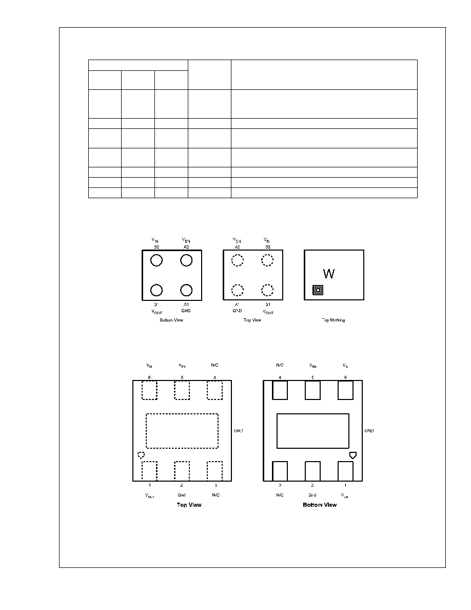
Pin Descriptions
Packages
Pin No
Symbol
Name and Function
LLP
micro
SMD
SOT23-5
5
A2
3
V
EN
Enable Input; Enables the Regulator when
0.95V.
Disables the Regulator when
0.4V.
Enable Input has 1M
pulldown resistor to GND.
2
A1
2
GND
Common Ground. Connect to Pad.
1
B1
5
V
OUT
Voltage output. A 0.47µF Low ESR Capacitor should be
connected to this Pin. Connect this output to the load circuit.
6
B2
1
V
IN
Voltage Supply Input. A 1.0µF capacitor should be connected
at this input.
3
4
N/C
No Connection. Do not connect to any other pin.
4
N/C
No Connection. Do not connect to any other pin.
Pad
GND
Common Ground. Connect to Pin 2.
Connection Diagrams
Micro SMD, 4 Bump Package
20076803
See NS package number TLA04
LLP-6 Package
20076806
See NS package number SDE06A
LP3990
www.national.com
2
Connection Diagrams
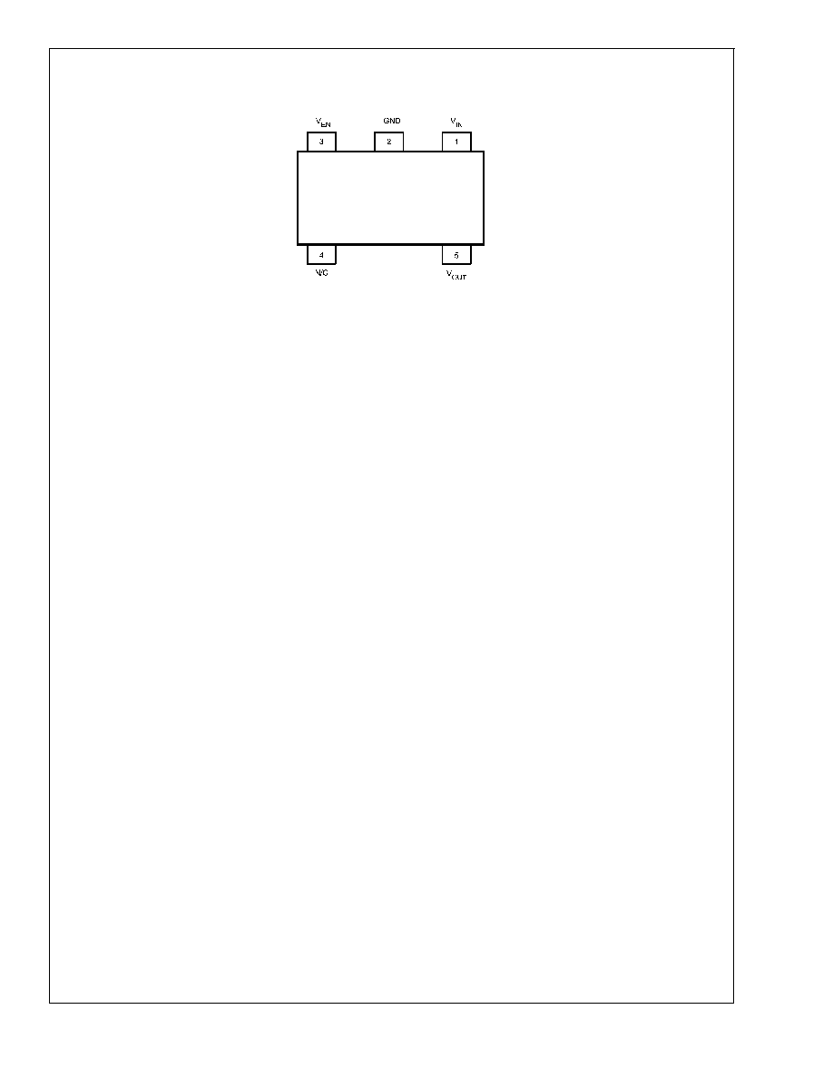
(Continued)
SOT23 - 5 Package (MF)
20076808
See NS package number MF05A
LP3990
www.national.com
3
Ordering Information
For micro SMD Package
* Please contact Sales Office for Availability
Output
Voltage (V)
Grade
LP3990 Supplied as 250
Units, Tape and Reel
LP3990 Supplied as 3000
Units, Tape and Reel
Package Marking
0.8
STD
LP3990TL-0.8
LP3990TLX-0.8
1.2*
STD
LP3990TL-1.2
LP3990TLX-1.2
1.35
STD
LP3990TL-1.35
LP3990TLX-1.35
1.5
STD
LP3990TL-1.5
LP3990TLX-1.5
1.8
STD
LP3990TL-1.8
LP3990TLX-1.8
2.5*
STD
LP3990TL-2.5
LP3990TLX-2.5
2.8
STD
LP3990TL-2.8
LP3990TLX-2.8
3.3*
STD
LP3990TL-3.3
LP3990TLX-3.3
For LLP-6 Package
* Please contact Sales Office for Availability
Output
Voltage (V)
Grade
LP3990 Supplied as 1000
Units, Tape and Reel
LP3990 Supplied as 3000
Units, Tape and Reel
Package Marking
0.8
STD
LP3990SD-0.8
LP3990SDX-0.8
L085B
1.2*
STD
LP3990SD-1.2
LP3990SDX-1.2
L086B
1.35*
STD
LP3990SD-1.35
LP3990SDX-1.35
L150B
1.5
STD
LP3990SD-1.5
LP3990SDX-1.5
L087B
1.8
STD
LP3990SD-1.8
LP3990SDX-1.8
L088B
2.5
STD
LP3990SD-2.5
LP3990SDX-2.5
L090B
2.8*
STD
LP3990SD-2.8
LP3990SDX-2.8
L091B
3.3*
STD
LP3990SD-3.3
LP3990SDX-3.3
L092B
For SOT23 - 5 Package
* Please contact Sales Office for Availability
Output
Voltage (V)
Grade
LP3990 Supplied as 1000
Units, Tape and Reel
LP3990 Supplied as 3000
Units, Tape and Reel
Package Marking
0.8*
STD
LP3990MF-0.8
LP3990MFX-0.8
SCCB
1.2*
STD
LP3990MF-1.2
LP3990MFX-1.2
SCDB
1.35*
STD
LP3990MF-1.35
LP3990MFX-1.35
SHRB
1.5*
STD
LP3990MF-1.5
LP3990MFX-1.5
SCEB
1.8*
STD
LP3990MF-1.8
LP3990MFX-1.8
SCFB
2.5*
STD
LP3990MF-2.5
LP3990MFX-2.5
SCJB
2.8*
STD
LP3990MF-2.8
LP3990MFX-2.8
SCKB
3.3*
STD
LP3990MF-3.3
LP3990MFX-3.3
SCLB
LP3990
www.national.com
4
Absolute Maximum Ratings
(Notes 1, 2)
If Military/Aerospace specified devices are required,
please contact the National Semiconductor Sales Office/
Distributors for availability and specifications.
Input Voltage
-0.3 to 6.5V
Output Voltage
-0.3 to (V
IN
+ 0.3V) to
6.5V (max)
Enable Input Voltage
-0.3 to (V
IN
+ 0.3V) to
6.5V (max)
Junction Temperature
150∞C
Lead/Pad Temp. (Note 3)
LLP/SOT23
235∞C
micro SMD
260∞C
Storage Temperature
-65 to 150∞C
Continuous Power Dissipation
Internally Limited(Note 4)
ESD (Note 5)
Human Body Model
2KV
Machine Model
200V
Operating Ratings
(Note 1)
Input Voltage
2V to 6V
Enable Input Voltage
0 to (V
IN
+ 0.3V) to
6.0V (max)
Junction Temperature
-40∞C to 125∞C
Ambient Temperature T
A
Range
(Note 6)
-40∞C to 85∞C
Thermal Properties
(Note 1)
Junction To Ambient Thermal
Resistance(Note 8)
JA
(LLP-6)
88∞C/W
JA
(microSMD)
220∞C/W
JA
SOT23-5
220∞C/W
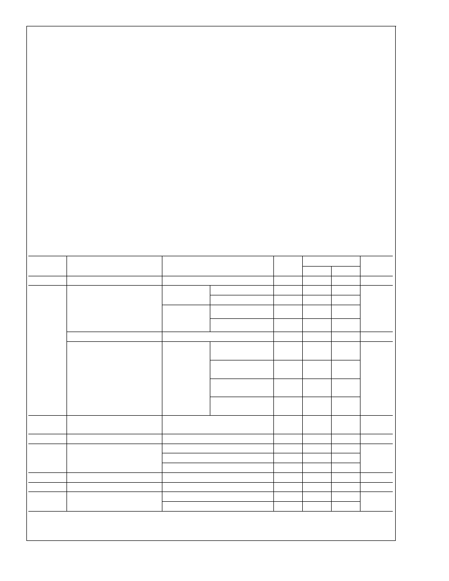
Electrical Characteristics
Unless otherwise noted, V
EN
=950mV, V
IN
= V
OUT
+ 1.0V, or 2.0V, whichever is higher. C
IN
= 1 µF, I
OUT
= 1 mA, C
OUT
=0.47
µF. Typical values and limits appearing in normal type apply for T
J
= 27∞C. Limits appearing in boldface type apply over the
full junction temperature range for operation, -40 to +125∞C. (Note 13)
Symbol
Parameter
Conditions
Typ
Limit
Units
Min
Max
V
IN
Input Voltage
(Note 14)
2
6
V
V
OUT
Output Voltage Tolerance
I
LOAD
= 1 mA
Micro SMD
-1
+1
%
LLP
-1.5
+1.5
Over full line
and load
regulation.
Micro SMD
-2.5
+2.5
LLP
-3
+3
Line Regulation Error
V
IN
= (V
OUT(NOM)
+ 1.0V) to 6.0V,
0.02
-0.1
0.1
%/V
Load Regulation Error
I
OUT
= 1mA
to 150mA
V
OUT
= 0.8 to 1.95V
MicroSMD
0.002
-0.005
0.005
%/mA
V
OUT
= 0.8 to 1.95V
LLP, SOT-23
0.003
-0.008
0.008
V
OUT
= 2.0 to 3.3V
MicroSMD
0.0005
-0.002
0.002
V
OUT
= 2.0 to 3.3V
LLP, SOT-23
0.002
-0.005
0.005
V
DO
Dropout Voltage
I
OUT
= 150mA
(Note 7)
120
mV
I
LOAD
Load Current
(Notes 9, 10)
0
µA
I
Q
Quiescent Current
V
EN
= 950mV, I
OUT
= 0mA
43
80
µA
V
EN
= 950mV, I
OUT
= 150mA
65
120
V
EN
= 0.4V
0.002
0.2
I
SC
Short Circuit Current Limit
(Note 11)
550
1000
mA
I
OUT
Maximum Output Current
150
mA
PSRR
Power Supply Rejection Ratio
f = 1kHz, I
OUT
= 1mA to 150mA
55
dB
f = 10kHz, I
OUT
= 150mA
35
LP3990
www.national.com
5