LP8358
150mA, µCap, Low Dropout Voltage Regulator with
Power Good
General Description
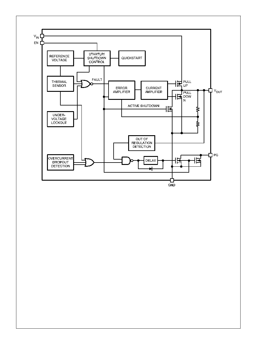
The LP8358 is a µCap, precise CMOS voltage regulator with
low Power good output R
DSON
.
It provides up to 150mA and consumes a typical of 10nA in
shutdown mode. The LP8358 output stage is designed with
a push pull output for faster transient recovery response.
The LP8358 is optimized to work with low value, low cost
ceramic capacitors. The output typically require only 1µF of
output capacitance for stability. The enable pin can be tied to
V
IN
for easy board layout.
The LP8358 is designed for portable, battery powered equip-
ment applications with small space requirements.
The LP8358 is available in a 5-pin SOT-23 package. Perfor-
mance is specified for the -40°C to +125°C temperature
range and is available in a fixed 1.2V. For other output
voltage options, please contact National Semiconductor.
Features
n
Low power good R
DSON
: 20
n
Power good indicator
n
Stability with low ESR capacitors
n
Low ground current: 120µA
n
150mA output current
n
"Zero" shutdown current mode
n
Fast transient recovery response
n
Auto discharge
n
Thermal shutdown
n
Current limiting
Applications
n
Processor power-up sequencing
n
Laptop, notebook and palm top computer
n
PCMCIA V
CC
and V
PP
regulation switching
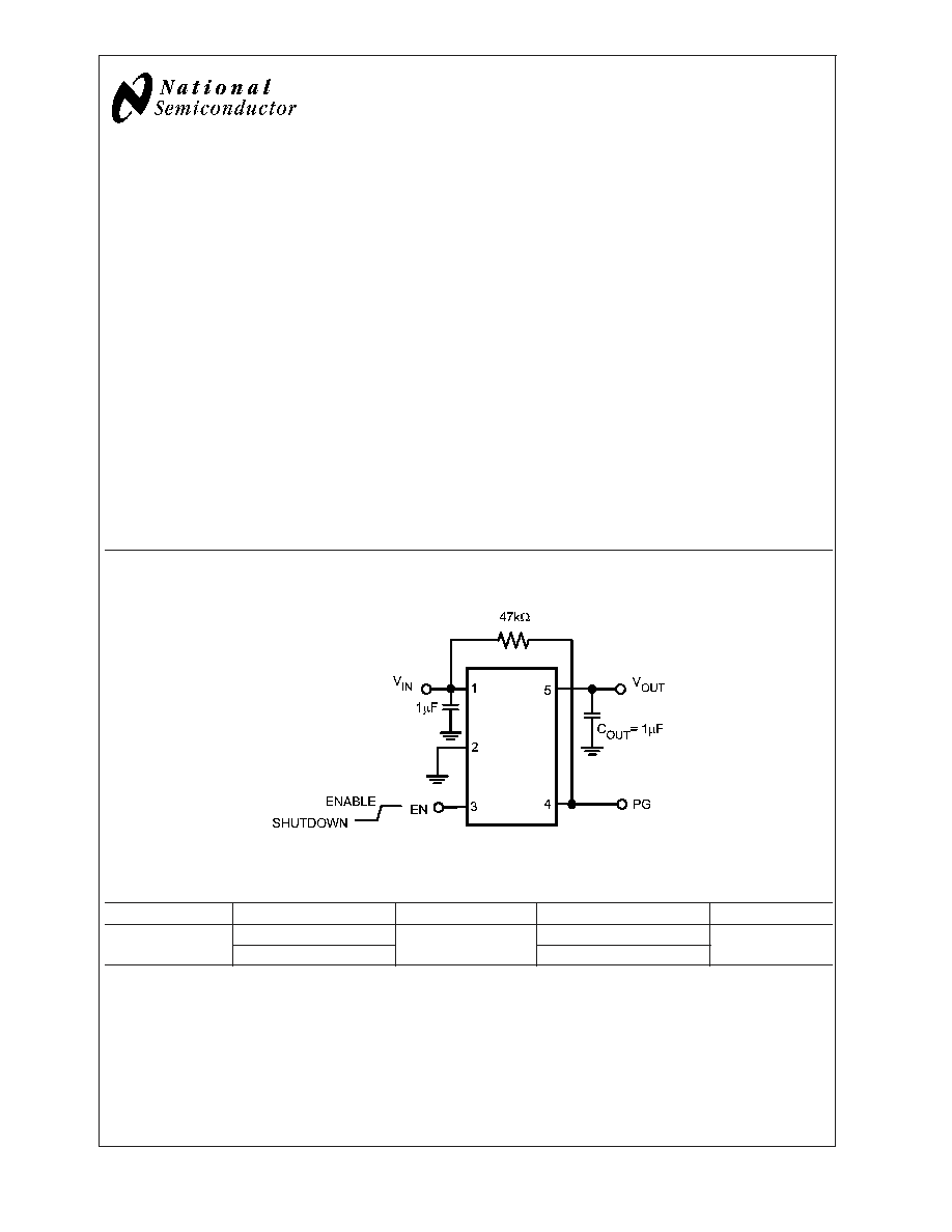
Typical Application
20057919
Ordering Information
Package
Part Number
Package Marking
Transport Media
NSC Drawing
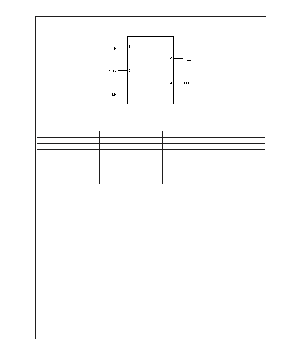
5-Pin SOT-23
LP8358MF-1.2
LH2B
1k Units Tape and Reel
MF05A
LP8358MFX-1.2
3k Units Tape and Reel
February 2003
LP8358
150mA,
µCap,
Low
Dropout
V
oltage
Regulator
with
Power
Good
© 2003 National Semiconductor Corporation
DS200579
www.national.com
Absolute Maximum Ratings
(Note 1)
If Military/Aerospace specified devices are required,
please contact the National Semiconductor Sales Office/
Distributors for availability and specifications.
ESD Tolerance (Note 2)
Human Body Model
2000V
Junction Temperature
150°C
V
IN
, V
OUT
, V
EN
-0.3 TO 6.5V
Soldering Information
Infrared or Convection (20 sec)
235°C
Wave Soldering (10 sec)
260°C (lead temp)
Operating Ratings
Supply Voltages
V
IN
2.7V to 6V
V
EN
0V to V
IN
Junction Temp. Range (Note 3)
-40°C to +125°C
Storage Temperature Range
-65°C to 150°C
Package Themal Resistance
SOT23-5
235°C/W
Electrical Characteristics
Unless otherwise specified, all limits guaranteed for T
J
= 25°C, V
IN
= 2.7V, I
L
= 100µA, C
OUT
= 1µF, V
EN
2.0V. Boldface
limits apply over the entire operating temperature range, -40°C to 125°C.
Symbol
Parameter
Conditions
Min
(Note 5)
Typ
(Note 4)
Max
(Note 5)
Units
V
O
Output Voltage Accuracy
I
L
= 100µA
-3
-4
3
4
%
V
O
/V
O
Line Regulation
V
IN
= 2.7V to 6V
-0.3
0.3
%
V
O
/V
O
Load Regulation
I
L
= 0.1mA to 150mA (Note 6)
1
4
%
I
Q
Quiescent Current
V
EN
0.4V (Shutdown), PG = NC
0.01
1
µA
I
GND
Ground Pin Current (Note 5)
I
L
= 0mA, V
EN
2.0V (active),
V
IN
= 6V
120
180
µA
I
L
= 150mA, V
EN
2.0V (active),
V
IN
= 6V
160
225
PSRR
Power Supply Rejection
Ratio
f = 120Hz, C
OUT
= 4.7µF,
I
L
= 150mA
62
dB
I
LIMIT
Current Limit
V
OUT
= 0V
160
350
mA
Thermal Protection
Thermal Shutdown
Temperature
150
°C
Enable Input
V
IL
Enable Input Voltage Level
Logic Low (off) , V
IN
= 5.5V
0.4
V
V
IH
Logic High (on), V
IN
= 5.5V
2
V
I
IL
Enable Input Current
V
IL
0.4V, V
IN
= 5.5V
0.01
µA
I
IH
V
IH
2.0V, V
IN
= 5.5V
0.01
µA
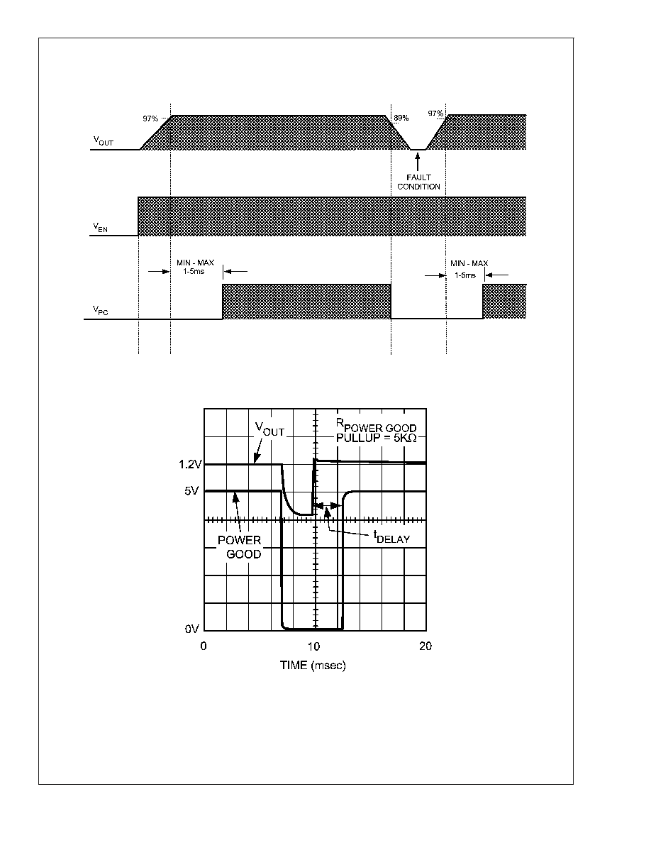
Power Good
V
PG
Low Threshold
% of V
OUT
(PG ON)
89
%
High Threshold
% of V
OUT
(PG OFF)
97
V
OL
PG Output Logic-Low
Voltage
I
POWERGOOD
= 100µA, Fault
Condition
2.0
10.0
mV
R
DSON
Power Good Output On -
Resistance
I
POWERGOOD
= 1mA, Fault Condition
20
I
PG
Power Good Leakage
Current
Power Good Off, V
PG
= 5.5V
0.01
µA
V
PG
Delay
Delay Time to Power Good
See Timing Diagram
1
2.1
5
ms
Note 1: Absolute Maximum Ratings indicate limits beyond which damage to the device may occur. Operating Ratings indicate conditions for which the device is
intended to be functional, but specific performance is not guaranteed. For guaranteed specifications and the test conditions, see the Electrical Characteristics.
Note 2: Human body model, 1.5k
in series with 100pF.
Note 3: The maximum power dissipation is a function of T
J(max)
,
JA
, and T
A
. The maximum allowable power dissipation at any ambient temperature
is P
D
= (T
J(max)
T
A
)/
JA
. All numbers apply for packages soldered directly into a PC board.
Note 4: Typical Values represent the most likely parametric norm.
Note 5: All limits are guaranteed by testing or statistical analysis.
Note 6: Regulation is measured at constant junction temperature using low duty cycle pulse testing.
LP8358
www.national.com
4
Electrical Characteristics
(Continued)
Note 7: Ground pin current is the regulator quiescent current. The total current drawn from the supply is the sum of the load current plus the ground pin current.
Timing Diagram
20057915
Typical delay time to power good
20057925
LP8358
www.national.com
5