TL C 5171
NSC800
High-Performance
Low-Power
CMOS
Microprocessor
June 1992
NSC800
TM
High-Performance
Low-Power CMOS Microprocessor
General Description
The NSC800 is an 8-bit CMOS microprocessor that func-
tions as the central processing unit (CPU) in National Semi-
conductor's NSC800 microcomputer family
National's
microCMOS technology used to fabricate this device pro-
vides system designers with performance equivalent to
comparable NMOS products but with the low power advan-
tage of CMOS Some of the many system functions incorpo-
rated on the device are vectored priority interrupts refresh
control power-save feature and interrupt acknowledge The
NSC800 is available in dual-in-line and surface mounted
chip carrier packages
The system designer can choose not only from the dedicat-
ed CMOS peripherals that allow direct interfacing to the
NSC800 but from the full line of National's CMOS products
to allow a low-power system solution The dedicated periph-
erals include NSC810A RAM I O Timer NSC858 UART
and NSC831 I O
All devices are available in commercial industrial and mili-
tary temperature ranges along with two added reliability
flows The first is an extended burn in test and the second is
the military class C screening in accordance with Method
5004 of MIL-STD-883
Features
Y
Fully compatible with Z80
instruction set
Powerful set of 158 instructions
10 addressing modes
22 internal registers
Y
Low power 50 mW at 5V V
CC
Y
Unique power-save feature
Y
Multiplexed bus structure
Y
Schmitt trigger input on reset
Y
On-chip bus controller and clock generator
Y
Variable power supply 2 4V
b
6 0V
Y
On-chip 8-bit dynamic RAM refresh circuitry
Y
Speed 1 0 ms instruction cycle at 4 0 MHz
NSC800-4
4 0 MHz
NSC800-35
3 5 MHz
NSC800-3
2 5 MHz
NSC800-1
1 0 MHz
Y
Capable of addressing 64k bytes of memory and 256
I O devices
Y
Five interrupt request lines on-chip
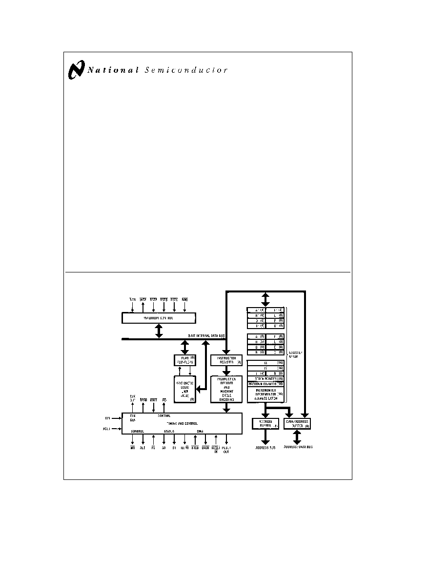
Block Diagram
TL C 5171 � 73
NSC800
TM
is a trademark of National Semiconductor Corp
TRI-STATE
is a registered trademark of National Semiconductor Corp
Z80
is a registered trademark of Zilog Corp
C1995 National Semiconductor Corporation
RRD-B30M105 Printed in U S A

Table of Contents
1 0 ABSOLUTE MAXIMUM RATINGS
2 0 OPERATING CONDITIONS
3 0 DC ELECTRICAL CHARACTERISTICS
4 0 AC ELECTRICAL CHARACTERISTICS
5 0 TIMING WAVEFORMS
NSC800 HARDWARE
6 0 PIN DESCRIPTIONS
6 1 Input Signals
6 2 Output Signals
6 3 Input Output Signals
7 0 CONNECTION DIAGRAMS
8 0 FUNCTIONAL DESCRIPTION
8 1 Register Array
8 2 Dedicated Registers
8 2 1 Program Counter
8 2 2 Stack Pointer
8 2 3 Index Register
8 2 4 Interrupt Register
8 2 5 Refresh Register
8 3 CPU Working and Alternate Register Sets
8 3 1 CPU Working Registers
8 3 2 Alternate Registers
8 4 Register Functions
8 4 1 Accumulator
8 4 2 F Register
Flags
8 4 3 Carry (C)
8 4 4 Adds Subtract (N)
8 4 5 Parity Overflow (P V)
8 4 6 Half Carry (H)
8 4 7 Zero Flag (Z)
8 4 8 Sign Flag (S)
8 4 9 Additional General Purpose Registers
8 4 10 Alternate Configurations
8 5 Arithmetic Logic Unit (ALU)
8 6 Instruction Register and Decoder
9 0 TIMING AND CONTROL
9 1 Internal Clock Generator
9 2 CPU Timing
9 3 Initialization
9 4 Power Save Feature
9 0 TIMING AND CONTROL
9 5 Bus Access Control
9 6 Interrupt Control
NSC800 SOFTWARE
10 0 INTRODUCTION
11 0 ADDRESSING MODES
11 1 Register
11 2 Implied
11 3 Immediate
11 4 Immediate Extended
11 5 Direct Addressing
11 6 Register Indirect
11 7 Indexed
11 8 Relative
11 9 Modified Page Zero
11 10 Bit
12 0 INSTRUCTION SET
12 1 Instruction Set Index Alphabetical
12 2 Instruction Set Mnemonic Notation
12 3 Assembled Object Code Notation
12 4 8-Bit Loads
12 5 16-Bit Loads
12 6 8-Bit Arithmetic
12 7 16-Bit Arithmetic
12 8 Bit Set Reset and Test
12 9 Rotate and Shift
12 10 Exchanges
12 11 Memory Block Moves and Searches
12 12 Input Output
12 13 CPU Control
12 14 Program Control
12 15 Instruction Set Alphabetical Order
12 16 Instruction Set Numerical Order
13 0 DATA ACQUISITION SYSTEM
14 0 NSC800M 883B MIL STD 883 CLASS C
SCREENING
15 0 BURN-IN CIRCUITS
16 0 ORDERING INFORMATION
17 0 RELIABILITY INFORMATION
2
1 0 Absolute Maximum Ratings
(Note 1)
If Military Aerospace specified devices are required
please contact the National Semiconductor Sales
Office Distributors for availability and specifications
Storage Temperature
b
65 C to
a
150 C
Voltage on Any Pin
with Respect to Ground
b
0 3V to V
CC
a
0 3V
Maximum V
CC
7V
Power Dissipation
1W
Lead Temp (Soldering 10 seconds)
300 C
2 0 Operating Conditions
NSC800-1
x
T
A
e
0 C to
a
70 C
T
A
e b
40 C to
a
85 C
NSC800-3
x
T
A
e
0 C to
a
70 C
T
A
e b
40 C to
a
85 C
T
A
e b
55 C to
a
125 C
NSC800-35 883C
x
T
A
e b
55 C to
a
125 C
NSC800-4
x
T
A
e
0 C to
a
70 C
T
A
e b
40 C to
a
85 C
NSC800-4MIL
x
T
A
e b
55 C to
a
90 C
3 0 DC Electrical Characteristics
V
CC
e
5V
g
10% GND
e
0V unless otherwise specified
Symbol
Parameter
Conditions
Min
Typ
Max
Units
V
IH
Logical 1 Input Voltage
0 8 V
CC
V
CC
V
V
IL
Logical 0 Input Voltage
0
0 2 V
CC
V
V
HY
Hysteresis at RESET IN input
V
CC
e
5V
0 25
0 5
V
V
OH1
Logical 1 Output Voltage
I
OUT
e b
1 0 mA
2 4
V
V
OH2
Logical 1 Output Voltage
I
OUT
e b
10 mA
V
CC
b
0 5
V
V
OL1
Logical 0 Output Voltage
I
OUT
e
2 mA
0
0 4
V
V
OL2
Logical 0 Output Voltage
I
OUT
e
10 mA
0
0 1
V
I
IL
Input Leakage Current
0
s
V
IN
s
V
CC
b
10 0
10 0
m
A
I
OL
Output Leakage Current
0
s
V
IN
s
V
CC
b
10 0
10 0
m
A
I
CC
Active Supply Current
I
OUT
e
0 f
(XIN)
e
2 MHz T
A
e
25 C
8
11
mA
I
CC
Active Supply Current
I
OUT
e
0 f
(XIN)
e
5 MHz T
A
e
25 C
10
15
mA
I
CC
Active Supply Current
I
OUT
e
0 f
(XIN)
e
7 MHz
15
21
mA
T
A
e
25 C
I
CC
Active Supply Current
I
OUT
e
0 f
(XIN)
e
8 MHz T
A
e
25 C
15
21
mA
I
Q
Quiescent Current
I
OUT
e
0 PS
e
0 V
IN
e
0 or V
IN
e
V
CC
2
5
mA
f
(XIN)
e
0 MHz T
A
e
25 C X
IN
e
0 CLK
e
1
I
PS
Power-Save Current
I
OUT
e
0 PS
e
0 V
IN
e
0 or V
IN
e
V
CC
5
7
mA
f
(XIN)
e
5 0 MHz T
A
e
25
C
IN
Input Capacitance
6
10
pF
C
OUT
Output Capacitance
8
12
pF
V
CC
Power Supply Voltage
(Note 2)
2 4
5
6
V
Note 1
Absolute Maximum Ratings indicate limits beyond which permanent damage may occur Continuous operation at these limits is not intended and should be
limited to those conditions specified under DC Electrical Characteristics
Note 2
CPU operation at lower voltages will reduce the maximum operating speed Operation at voltages other than 5V
g
10% is guaranteed by design not
tested
3
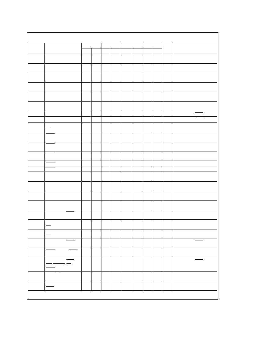
4 0 AC Electrical Characteristics
V
CC
e
5V
g
10% GND
e
0V unless otherwise specified
Symbol
Parameter
NSC800-1
NSC800-3
NSC800-35
NSC800-4
Units
Notes
Min
Max
Min
Max
Min
Max
Min
Max
t
X
Period at XIN and XOUT
500
3333 200 3333
142
3333
125 3333
ns
Pins
T
Period at Clock Output
1000 6667 400 6667
284
6667
250 6667
ns
(
e
2 t
X
)
t
R
Clock Rise Time
110
110
90
80
ns
Measured from
10% � 90% of signal
t
F
Clock Fall Time
70
60
55
50
ns
Measured from
10% � 90% of signal
t
L
Clock Low Time
435
150
90
80
ns
50% duty cycle square
wave input on XIN
t
H
Clock High Time
450
145
85
75
ns
50% duty cycle square
wave input on XIN
t
ACC(OP)
ALE to Valid Data
1340
490
340
300
ns
Add t for each WAIT STATE
t
ACC(MR)
ALE to Valid Data
1875
620
405
360
ns
Add t for each WAIT STATE
t
AFR
AD(0 � 7) Float after
0
0
0
0
ns
RD Falling
t
BABE
BACK Rising to Bus
1000
400
300
250
ns
Enable
t
BABF
BACK Falling to
50
50
50
50
ns
Bus Float
t
BACL
BACK Fall to CLK
425
125
60
55
ns
Falling
t
BRH
BREQ Hold Time
0
0
0
0
ns
t
BRS
BREQ Set-Up Time
100
50
50
45
ns
t
CAF
Clock Falling ALE
0
70
0
65
0
60
0
55
ns
Falling
t
CAR
Clock Rising to ALE
0
100
0
100
0
90
0
80
ns
Rising
t
CRD
Clock Rising to
100
90
90
80
ns
Read Rising
t
CRF
Clock Rising to
80
70
70
65
ns
Refresh Falling
t
DAI
ALE Falling to INTA
445
160
95
85
ns
Falling
t
DAR
ALE Falling to
400
575
160
250
100
180
90
160
ns
RD Falling
t
DAW
ALE Falling to
900
1010 350
420
225
300
200
265
ns
WR Falling
t
D(BACK)1
ALE Falling to BACK
2460
975
635
560
ns
Add t for each WAIT state
Falling
Add t for opcode fetch cycles
t
D(BACK)2
BREQ Rising to BACK
500
1610 200
700
140
540
125
475
ns
Rising
t
D(I)
ALE Falling to INTR
1360
475
284
250
ns
Add t for each WAIT state
NMI RSTA-C PS
Add t for opcode fetch cycles
BREQ Inputs Valid
t
DPA
Rising PS to
500
1685 200
760
140
580
125
510
ns
See
Figure 14 also
Falling ALE
t
D(WAIT)
ALE Falling to
550
250
170
125
ns
WAIT Input Valid
OP
Opcode Fetch
MR
Memory Read
4
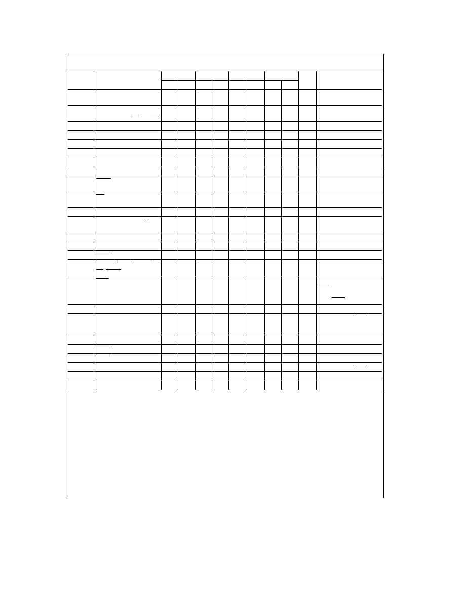
4 0 AC Electrical Characteristics
V
CC
e
5V
g
10% GND
e
0V unless otherwise specified (Continued)
Symbol
Parameter
NSC800-1
NSC800-3
NSC800-35
NSC800-4
Units
Notes
Min
Max
Min
Max
Min
Max
Min
Max
T
H(ADH)1
A(8 � 15) Hold Time During
0
0
0
0
ns
Opcode Fetch
T
H(ADH)2
A(8 � 15) Hold Time During
400
100
85
60
ns
Memory or IO RD and WR
T
H(ADL)
AD(0 � 7) Hold Time
100
60
35
30
ns
T
H(WD)
Write Data Hold Time
400
100
85
75
ns
t
INH
Interrupt Hold Time
0
0
0
0
ns
t
INS
Interrupt Set-Up Time
100
50
50
45
ns
t
NMI
Width of NMI Input
50
30
25
20
ns
t
RDH
Data Hold after Read
0
0
0
0
ns
t
RFLF
RFSH Rising to ALE
60
50
45
40
ns
Falling
t
RL(MR)
RD Rising to ALE Rising
390
100
50
45
ns
(Memory Read)
t
S(AD)
AD(0 � 7) Set-Up Time
300
45
45
40
ns
t
S(ALE)
A(8 � 15) SO SI IO M
350
70
55
50
ns
Set-Up Time
t
S(WD)
Write Data Set-Up Time
385
75
35
30
ns
t
W(ALE)
ALE Width
430
130
115
100
ns
t
WH
WAIT Hold Time
0
0
0
0
ns
t
W(I)
Width of INTR RSTA-C
500
200
140
125
ns
PS BREQ
t
W(INTA)
INTA Strobe Width
1000
400
225
200
ns
Add two t states for first
INTA of each interrupt
response string Add t for
each WAIT state
t
WL
WR Rising to ALE Rising
450
130
70
70
ns
t
W(RD)
Read Strobe Width During
960
360
210
185
ns
Add t for each WAIT
State Add t 2 for Memory
Opcode Fetch
Read Cycles
t
W(RFSH)
Refresh Strobe Width
1925
725
450
395
ns
t
WS
WAIT Set-Up Time
100
70
60
55
ns
t
W(WAIT)
WAIT Input Width
550
250
195
175
ns
t
W(WR)
Write Strobe Width
985
370
250
220
ns
Add t for each WAIT state
t
XCF
XIN to Clock Falling
25
100
15
95
5
90
5
80
ns
t
XCR
XIN to Clock Rising
25
85
15
85
5
90
5
80
ns
Note 1
Test conditions t
e
1000 ns for NSC800-1 400 ns for NSC800 285 ns for NSC800-35 250 ns for NSC800-4
Note 2
Output timings are measured with a purely capacitive load of 100 pF
5