TL F 11657
SCAN182245A
Transceiver
with
25
X
Series
Resistor
Outputs
February 1996
SCAN182245A
Non-Inverting Transceiver with
25X Series Resistor Outputs
General Description
The SCAN182245A is a high performance BiCMOS bidirec-
tional line driver featuring separate data inputs organized
into dual 9-bit bytes with byte-oriented output enable and
direction control signals This device is compliant with
IEEE 1149 1 Standard Test Access Port and Boundary
Scan Architecture with the incorporation of the defined
boundary-scan test logic and test access port consisting of
Test Data Input (TDI) Test Data Out (TDO) Test Mode Se-
lect (TMS) and Test Clock (TCK)
Features
Y
High performance BiCMOS technology
Y
25X series resistors in outputs eliminate the need for
external terminating resistors
Y
Dual output enable control signals
Y
TRI-STATE
outputs for bus-oriented applications
Y
25 mil pitch SSOP (Shrink Small Outline Package)
Y
IEEE 1149 1 (JTAG) Compliant
Y
Includes CLAMP IDCODE and HIGHZ instructions
Y
Additional instructions SAMPLE-IN SAMPLE-OUT and
EXTEST-OUT
Y
Power Up TRI-STATE for hot insert
Y
Member of National's SCAN Products
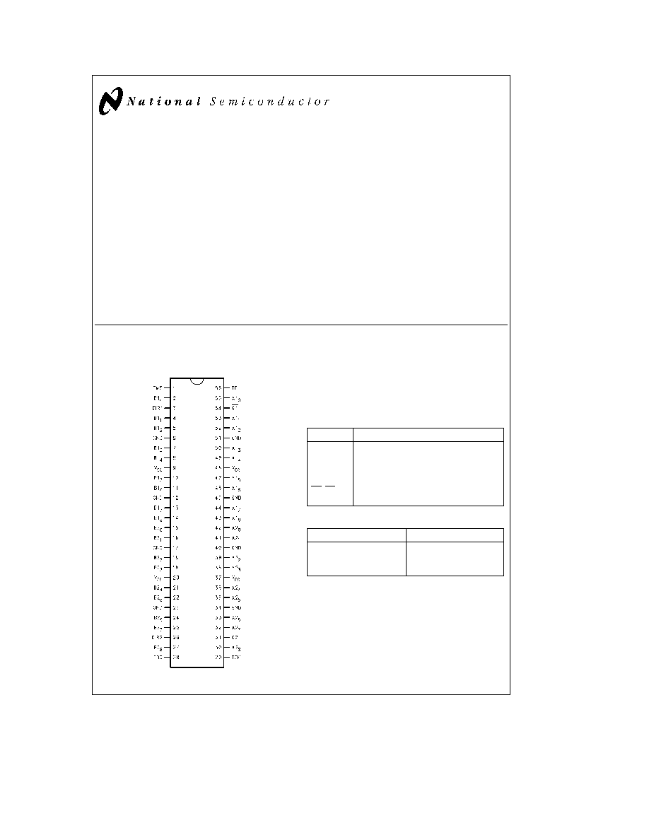
Connection Diagram
TL F 11657 ≠ 1
Pin Names
Description
A1
(0 ≠ 8)
Side A1 Inputs or TRI-STATE Outputs
B1
(0 ≠ 8)
Side B1 Inputs or TRI-STATE Outputs
A2
(0 ≠ 8)
Side A2 Inputs or TRI-STATE Outputs
B2
(0 ≠ 8)
Side B2 Inputs or TRI-STATE Outputs
G1 G2
Output Enable Pins (Active Low)
DIR1 DIR2
Direction of Data Flow Pins
Order Number
Description
SCAN182245ASSC
SSOP in Tubes
SCAN182245ASSCX
SSOP Tape and Reel
SCAN182245AFMQB
Flatpak Military
TRI-STATE
is a registered trademark of National Semiconductor Corporation
C1996 National Semiconductor Corporation
RRD-B30M36 Printed in U S A
http
www national com
Truth Tables
Inputs
A1
(0 ≠ 8)
B1
(0 ≠ 8)
G1
DIR1
L
L
H
w
H
L
L
L
w
L
L
H
H
x
H
L
H
L
x
L
H
X
Z
Z
Inputs
A2
(0 ≠ 8)
B2
(0 ≠ 8)
G2
DIR2
L
L
H
w
H
L
L
L
w
L
L
H
H
x
H
L
H
L
x
L
H
X
Z
Z
H
e
HIGH Voltage Level
L
e
LOW Voltage Level
X
e
Immaterial
Z
e
High Impedance
e
Inactive-to-Active transition must occur to enable outputs upon
power-up
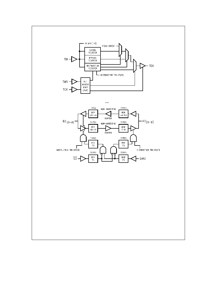
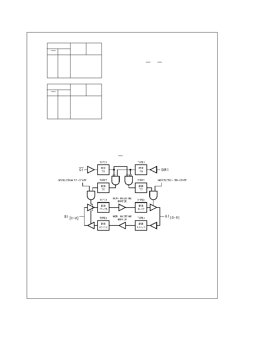
Functional Description
The SCAN182245A consists of two sets of nine non-invert-
ing bidirectional buffers with TRI-STATE outputs and is in-
tended for bus-oriented applications Direction pins (DIR1
and DIR2) LOW enables data from B ports to A ports when
HIGH enables data from A ports to B ports The Output
Enable pins (G1 and G2) when HIGH disables both A and B
ports by placing them in a high impedance condition
Block Diagrams
A1 B1 G1 and DIR1
TL F 11657 ≠ 2
Note
BSR stands for Boundary Scan Register
http
www national com
2
Description of BOUNDARY-SCAN Circuitry
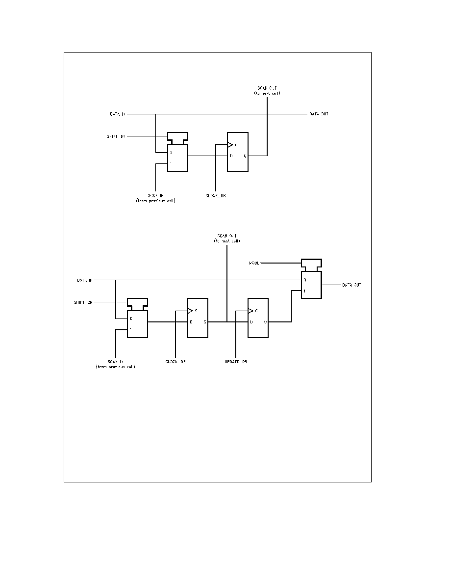
The scan cells used in the BOUNDARY-SCAN register are
one of the following two types depending upon their loca-
tion Scan cell TYPE1 is intended to solely observe system
data while TYPE2 has the additional ability to control sys-
tem data (See IEEE Standard 1149 1
Figure 10-11 for a
further description of scan cell TYPE1 and
Figure 10-12 for
a further description of scan cell TYPE2 )
Scan cell TYPE1 is located on each system input pin while
scan cell TYPE2 is located at each system output pin as
well as at each of the two internal active-high output enable
signals AOE controls the activity of the A-outputs while
BOE controls the activity of the B-outputs Each will activate
their respective outputs by loading a logic high
The BYPASS register is a single bit shift register stage iden-
tical to scan cell TYPE1 It captures a fixed logic low
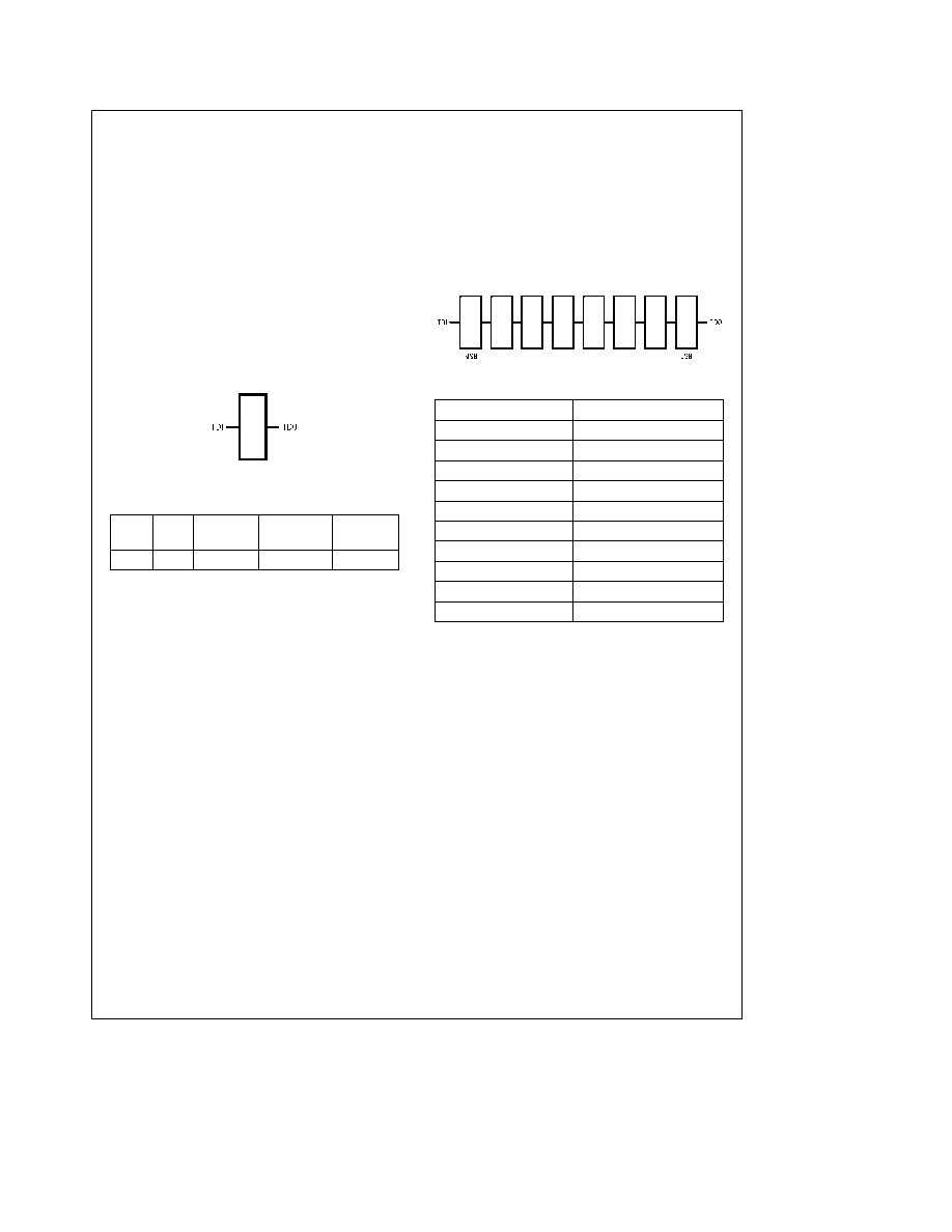
Bypass Register Scan Chain Definition
Logic 0
TL F 11657 ≠ 17
SCAN182245A Product IDCODE
(32-Bit Code per IEEE 1149 1)
Version Entity
Part
Manufacturer Required by
Number
ID
1149 1
0000
111111 0000000000 00000001111
1
MSB
LSB
The INSTRUCTION register is an 8-bit register which cap-
tures the default value of 10000001 (SAMPLE PRELOAD)
during the CAPTURE-IR instruction command The benefit
of capturing SAMPLE PRELOAD as the default instruction
during CAPTURE-IR is that the user is no longer required to
shift in the 8-bit instruction for SAMPLE PRELOAD The se-
quence of CAPTURE-IR
x
EXIT1-IR
x
UPDATE-IR
will update the SAMPLE PRELOAD instruction For more
information refer to the section on instruction definitions
Instruction Register Scan Chain Definition
TL F 11657 ≠ 10
MSB
x
LSB
Instruction Code
Instruction
00000000
EXTEST
10000001
SAMPLE PRELOAD
10000010
CLAMP
00000011
HIGH-Z
01000001
SAMPLE-IN
01000010
SAMPLE-OUT
00100010
EXTEST-OUT
10101010
IDCODE
11111111
BYPASS
All Others
BYPASS
http
www national com
4