CLC021
SMPTE 259M Digital Video Serializer with EDH
Generation and Insertion
General Description
The CLC021 SMPTE 259M Digital Video Serializer with EDH
Generation and Insertion is a monolithic integrated circuit
that encodes, serializes and transmits bit-parallel digital data
conforming to SMPTE 125M and 267M component video
and SMPTE 244M composite video standards. The CLC021
can also serialize other 8- or 10-bit parallel data. The
CLC021 operates at data rates from below 100 Mbps to over
400 Mbps. The serial data clock frequency is internally gen-
erated and requires no external frequency setting, trimming
or filtering components*.
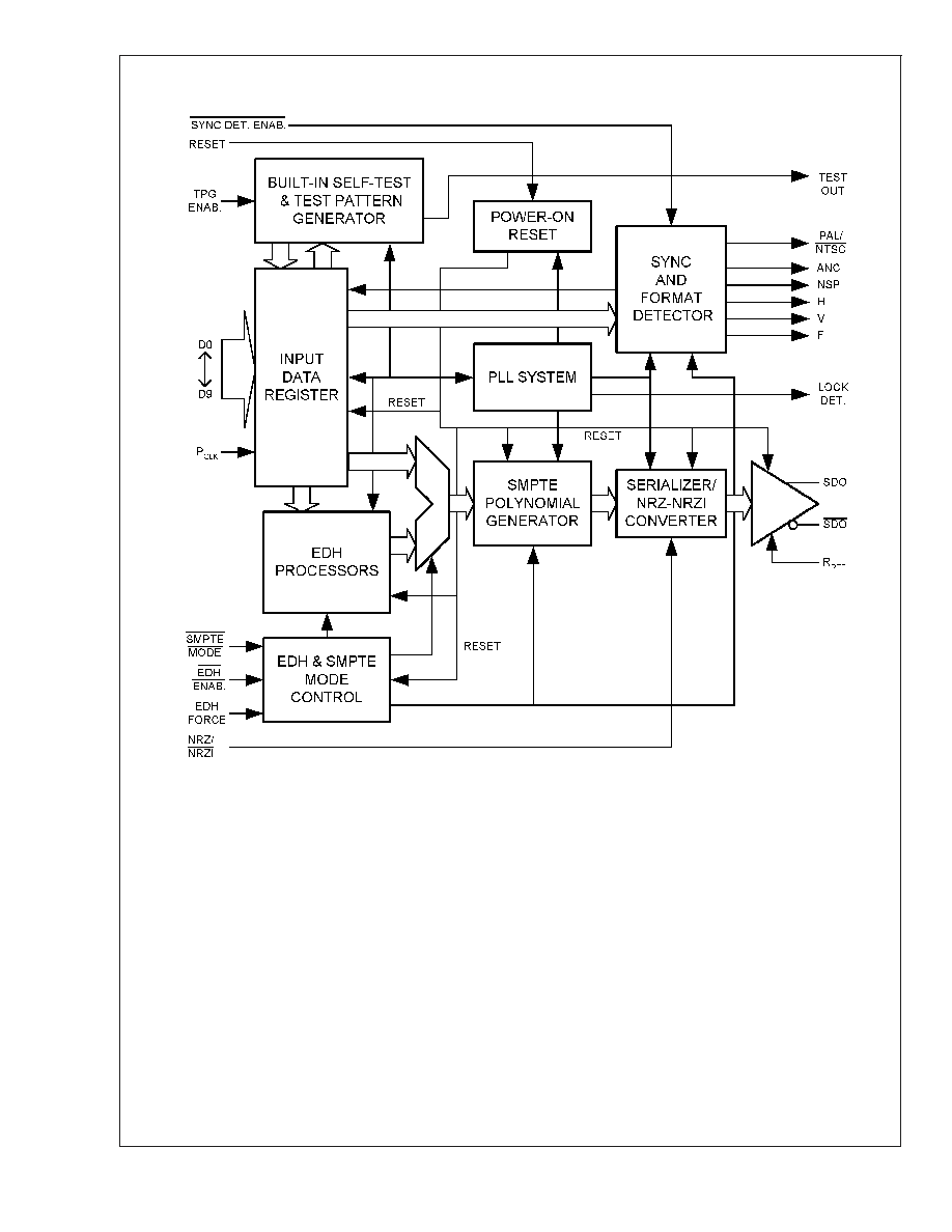
Functions performed by the CLC021 include: parallel-to-
serial data conversion, ITU-R BT.601-4 input data clipping,
data encoding using the SMPTE polynomial (X
9
+X
4
+1), data
format conversion from NRZ to NRZI, parallel data clock
frequency multiplication and encoding with the serial data,
and differential, serial output data driving. The CLC021 has
circuitry for automatic EDH character and flag generation
and insertion per SMPTE RP-165. The CLC021 has an
exclusive built-in self-test (BIST) and video test pattern gen-
erator (TPG) with 16 component video test patterns: refer-
ence black, PLL and EQ pathologicals and modified colour
bars in 4:3 and 16:9 raster formats for NTSC and PAL
formats*.
The CLC021 has inputs for enabling sync detection, non-
SMPTE mode operation, enabling the EDH function, NRZ/
NRZI mode control and an external reset control. Outputs
are provided for H, V and F bits, new TRS sync character
position indication, ancilliary data header detection, NTSC/
PAL raster indication and PLL lock detect. Separate power
pins for the output driver, VCO and the serializer improve
power supply rejection, output jitter and noise performance.
The CLC021AVGZ-5.0V is powered by a single +5V supply.
The CLC021AVGZ-3.3V is powered by a single +3.3V sup-
ply. Power dissipation is typically 235 mW including two 75
back-matched output loads. The device is packaged in a
JEDEC metric 44-lead PQFP.
Features
n
SMPTE 259M serial digital video standard compliant
n
Supports all NTSC and PAL standard component and
composite serial video data rates
n
No external serial data rate setting or VCO filtering
components required
*
n
Fast VCO lock time:
<
75 µs at 270 Mbps
n
Built-in self-test (BIST) and video test pattern generator
(TPG) with 16 internal patterns
*
n
Automatic EDH character and flag generation and
insertion per SMPTE RP 165
n
Non-SMPTE mode operation as parallel-to-serial
converter
n
NRZ-to-NRZI conversion control
n
HCMOS/LSTTL-compatible data and control inputs and
outputs for CLC021AVGZ-5.0, LVCMOS for
CLC021AVGZ-3.3
n
75
ECL-compatible, differential, serial cable-driver
outputs
n
Single power supply operation: 5V (CLC021AVGZ-5.0)
or 3.3V (CLC021AVGZ-3.3) in TTL or ECL systems
n
Low power: typically 235 mW
n
JEDEC 44-lead metric PQFP package
n
Commercial temperature range 0∞C to +70∞C
*
Patents applications made or pending.
Applications
n
SMPTE 259M parallel-to-serial digital video interfaces
for:
-- Video cameras
-- VTRs
-- Telecines
-- Video test pattern generators and digital video test
equipment
-- Video signal generators
n
Non-SMPTE video applications
n
Other high data rate parallel/serial video and data
applications
Typical Application
10136812
July 2003
CLC021
SMPTE
259M
Digital
V
ideo
Serializer
with
EDH
Generation
and
Insertion
© 2003 National Semiconductor Corporation
DS101368
www.national.com

Absolute Maximum Ratings
(Note 1) It
is anticipated that this device will not be offered in a
military qualified version. If Military/Aerospace speci-
fied devices are required, please contact the National
Semiconductor Sales Office / Distributors for availabil-
ity and specifications.
Supply Voltage (V
DD
-V
SS
):
CLC021AVGZ-5.0V
6.0V
CLC021AVGZ-3.3V
4.0V
CMOS/TTL Input Voltage (V
I
):
CLC021AVGZ-5.0V
-0.5V to V
DD
+0.5V
CLC021AVGZ-3.3V
-0.3V to V
DD
+0.3V
CMOS/TTL Output Voltage (V
O
):
CLC021AVGZ-5.0V
-0.5V to V
DD
+0.5V
CLC021AVGZ-3.3V
-0.3V to V
DD
+0.3V
CMOS/TTL Input Current (single input):
V
I
= V
SS
-0.5V:
-5 mA
V
I
= V
DD
+0.5V:
+5 mA
Input Current, Other Inputs:
±
1 mA
CMOS/TTL Output Source/Sink Current:
±
16 mA
SDO Output Source Current:
22 mA
Package Thermal Resistance
JA
44-lead Metric PQFP:
(
@
0 LFM airflow)
60∞C/W
(
@
500 LFM airflow)
43∞C/W
JC
44-lead Metric PQFP:
17∞C/W
Storage Temp. Range:
-65∞C to +150∞C
Junction Temperature:
+150∞C
Lead Temperature (Soldering 4
Sec):
+260∞C
ESD Rating (HBM):
2 kV
ESD Rating (MM):
150V
Transistor Count:
33,400
Recommended Operating
Conditions
Supply Voltage (V
DD
-V
SS
):
CLC021AVGZ-5.0
5.0V
±
10%
CLC021AVGZ-3.3
3.3V
±
10%
CMOS/TTL Input Voltage:
V
SS
to V
DD
Maximum DC Bias on SDO pins:
CLC021AVGZ-5.0
3.0V
±
10%
CLC021AVGZ-3.3
1.3V
±
10%
P
CLK
Frequency Range
10 to 40MHz
P
CLK
Duty Cycle
45 to 55%
D
N
and P
CLK
Rise/Fall Time
1.0 to 3.0 ns
Operating Free Air Temperature
(T
A
):
0∞C to +70∞C
DC Electrical Characteristics--CLC021AVGZ-5.0
Over Supply Voltage and Operating Temperature ranges, unless otherwise specified (Notes 2, 3).
Symbol
Parameter
Conditions
Reference
Min
Typ
Max
Units
V
IH
Input Voltage High Level
All CMOS Inputs
2.0
V
DD
V
V
IL
Input Voltage Low Level
V
SS
0.8
V
I
IH
Input Current High Level
V
IH
= V
DD
+40
+60
µA
I
IL
Input Current Low Level
V
IL
= V
SS
-1
-20
µA
V
OH
CMOS Output Voltage
High Level
I
OH
= -10 mA
All CMOS
Outputs
2.4
4.7
V
DD
V
V
OL
CMOS Output Voltage
Low Level
I
OL
= +10 mA
0.0
0.3
V
SS
+ 0.5V
V
V
SDO
Serial Driver Output
Voltage
R
L
= 75
1%,
R
REF
= 1.69 k
1%,
Figure 2
SDO, SDO
700
800
900
mV
P-P
I
DD
Power Supply Current,
Total
R
L
= 75
1%,
R
REF
= 1.69 k
1%,
P
CLK
= 27 MHz, NTSC
Colour Bar Pattern,
Figure 2
47
60
mA
DC Electrical Characteristics--CLC021AVGZ-3.3
Over Supply Voltage and Operating Temperature ranges, unless otherwise specified (Notes 2, 3).
Symbol
Parameter
Conditions
Reference
Min
Typ
Max
Units
V
IH
Input Voltage High Level
All CMOS Inputs
2.0
V
DD
V
V
IL
Input Voltage Low Level
V
SS
0.6
V
I
IH
Input Current High Level
V
IH
= V
DD
+22
+60
µA
I
IL
Input Current Low Level
V
IL
= V
SS
-1
-20
µA
CLC021
www.national.com
4

DC Electrical Characteristics--CLC021AVGZ-3.3
(Continued)
Over Supply Voltage and Operating Temperature ranges, unless otherwise specified (Notes 2, 3).
Symbol
Parameter
Conditions
Reference
Min
Typ
Max
Units
V
OH
CMOS Output Voltage
High Level
I
OH
= -8 mA
All CMOS
Outputs
2.4
3.0
V
DD
V
V
OL
CMOS Output Voltage
Low Level
I
OL
= +8 mA
0.0
0.3
V
SS
+ 0.5V
V
V
SDO
Serial Driver Output
Voltage
R
L
= 75
1%,
R
REF
= 1.69 k
1%,
Figure 2
SDO, SDO
720
800
880
mV
P-P
I
DD
Power Supply Current,
Total
R
L
= 75
1%,
R
REF
= 1.69 k
1%,
P
CLK
= 27 MHz, NTSC
Colour Bar Pattern,
Figure 2
33
55
mA
AC Electrical Characteristics--CLC021AVGZ-5.0
Over Supply Voltage and Operating Temperature ranges, unless otherwise specified (Note 3).
Symbol
Parameter
Conditions
Reference
Min
Typ
Max
Units
BR
SDO
Serial Data Rate
(Note 5)
SDO, SDO
100
400
Mbps
F
PCLK
Reference Clock
Input Frequency
P
CLK
10
40
MHz
Reference Clock Duty
Cycle
P
CLK
45
50
55
%
t
r
, t
f
Rise Time, Fall Time
D
N
, P
CLK
1.0
1.5
3.0
ns
t
j
Serial Output Jitter
270 Mbps,Figure 2, (Note 6)
SDO, SDO
220
ps
P-P
t
jit
Serial Output Jitter
(Notes 4, 5)
100
200
ps
P-P
t
r
, t
f
Rise Time, Fall Time
20%≠80%, (Notes 4, 5)
500
800
1500
ps
Output Overshoot
(Note 4)
1
%
t
LOCK
Lock Time
(Notes 5, 7)
75
µs
t
SU
Setup Time
Figure 3 (Note 4)
D
N
to P
CLK
3
2
ns
t
HLD
Hold Time
Figure 3 (Note 4)
D
N
from P
CLK
3
2
ns
L
GEN
Output Inductance
(Note 4)
SDO, SDO
6
nH
R
GEN
Output Resistance
(Note 4)
25k
AC Electrical Characteristics--CLC021AVGZ-3.3
Over Supply Voltage and Operating Temperature ranges, unless otherwise specified (Note 3).
Symbol
Parameter
Conditions
Reference
Min
Typ
Max
Units
BR
SDO
Serial Data Rate
(Note 5)
SDO, SDO
100
400
Mbps
F
PCLK
Reference Clock
Input Frequency
P
CLK
10
40
MHz
Reference Clock Duty
Cycle
P
CLK
45
50
55
%
t
r
, t
f
Rise Time, Fall Time
D
N
, P
CLK
1.0
1.5
3.0
ns
t
j
Serial Output Jitter
270 Mbps,Figure 2, (Note 6)
SDO, SDO
220
ps
P-P
t
jit
Serial Output Jitter
(Notes 4, 5)
100
200
ps
P-P
t
r
, t
f
Rise Time, Fall Time
20%≠80%, (Notes 4, 5)
500
800
1500
ps
Output Overshoot
(Note 4)
1
%
t
LOCK
Lock Time
(Notes 5, 7)
75
µs
t
SU
Setup Time
Figure 3 (Note 4)
D
N
to P
CLK
4
2
ns
t
HLD
Hold Time
Figure 3 (Note 4)
D
N
from P
CLK
4
2
ns
CLC021
www.national.com
5