 | –≠–ª–µ–∫—Ç—Ä–æ–Ω–Ω—ã–π –∫–æ–º–ø–æ–Ω–µ–Ω—Ç: TP3040AV | –°–∫–∞—á–∞—Ç—å:  PDF PDF  ZIP ZIP |
TL H 6660
TP3040
TP3040A
PCM
Monolithic
Filter
September 1994
TP3040 TP3040A PCM Monolithic Filter
General Description
The TP3040 TP3040A filter is a monolithic circuit contain-
ing both transmit and receive filters specifically designed for
PCM CODEC filtering applications in 8 kHz sampled sys-
tems
The filter is manufactured using microCMOS technology
and switched capacitor integrators are used to simulate
classical LC ladder filters which exhibit low component sen-
sitivity
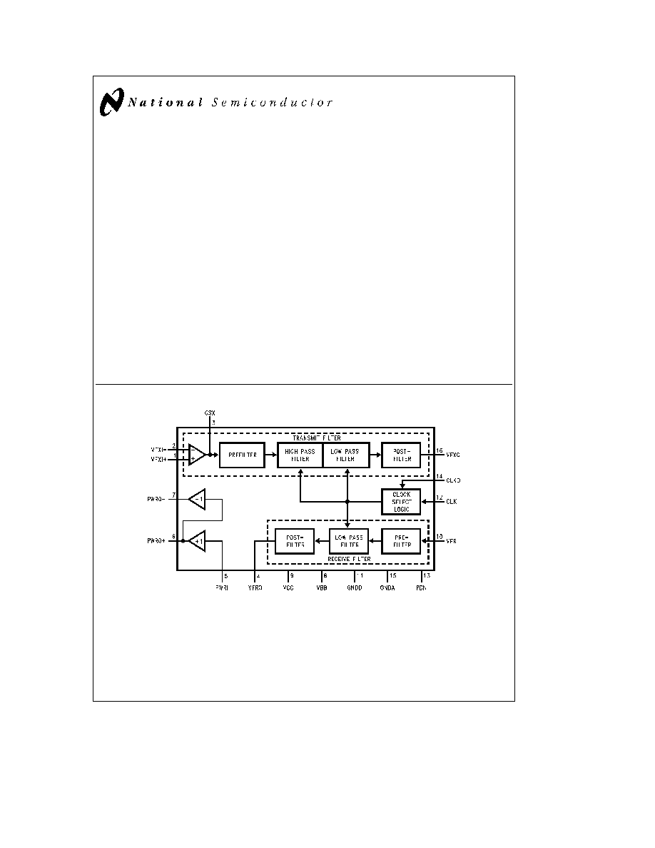
TRANSMIT FILTER STAGE
The transmit filter is a fifth order elliptic low pass filter in
series with a fourth order Chebyshev high pass filter It pro-
vides a flat response in the passband and rejection of sig-
nals below 200 Hz and above 3 4 kHz
RECEIVE FILTER STAGE
The receive filter is a fifth order elliptic low pass filter de-
signed to reconstruct the voice signal from the decoded de-
multiplexed signal which as a result of the sampling pro-
cess is a stair-step signal having the inherent sin x x fre-
quency response The receive filter approximates the func-
tion required to compensate for the degraded frequency re-
sponse and restore the flat passband response
Features
Y
Designed for D3 D4 and CCITT applications
Y
a
5V
b
5V power supplies
Y
Low power consumption
45 mW (0 dBm0 into 600X)
30 mW (power amps disabled)
Y
Power down mode 0 5 mW
Y
20 dB gain adjust range
Y
No external anti-aliasing components
Y
Sin x x correction in receive filter
Y
50 60 Hz rejection in transmit filter
Y
TTL and CMOS compatible logic
Y
All inputs protected against static discharge due to
handling
Block Diagram
TL H 6660 ≠ 1
FIGURE 1
C1995 National Semiconductor Corporation
RRD-B30M115 Printed in U S A
Absolute Maximum Ratings
If Military Aerospace specified devices are required
please contact the National Semiconductor Sales
Office Distributors for availability and specifications
Supply Voltages
g
7V
Power Dissipation
1 W Package
Input Voltage
g
7V
Voltage at Any Input
or Output
V
CC
a
0 3V to V
BBV
b
0 3V
Output Short-Circuit Duration
Continuous
Operating Temperature Range
b
25 C to
a
125 C
Storage Temperature
b
65 C to
a
150 C
Lead Temperature (Soldering 10 seconds)
300 C
ESD Rating to be determined
DC Electrical Characteristics
Unless otherwise noted limits printed in BOLD characters are guaranteed for
V
CC
e a
5 0V
g
5% V
BB
e b
5 0V
g
5% T
A
e
0 C to 70 C by correlation with 100% electrical testing at T
A
e
25 C All other
limits are assured by correlation with other production tests and or product design and characterization Typicals specified at
V
CC
e a
5 0V V
BB
e b
5 0V T
A
e
25 C Clock frequency is 2 048 MHz Digital interface voltages measured with respect to
digital ground GNDD Analog voltages measured with respect to analog ground GNDA
Symbol
Parameter
Conditions
Min
Typ
Max
Units
POWER DISSIPATION
I
CC0
V
CC
Standby Current
V
CC
e
5 25V V
BB
e b
5 25V
CLK0 and PWRI
e b
5 25V (Note 6)
50
100
m
A
All other pins at GND (0V)
TP3040 TP3040A
I
BB0
V
BB
Standby Current
V
CC
e
5 25V V
BB
e b
5 25V
CLK0 and PWRI
e b
5 25V (Note 6)
50
100
m
A
All other pins at GND (0V)
TP3040 TP3040A
I
CC1
V
CC
Operating Current
PWRI
e
V
BB
Power Amp Inactive
3 0
4 0
mA
I
BB1
V
BB
Operating Current
PWRI
e
V
BB
Power Amp Inactive
3 0
4 0
mA
I
CC2
V
CC
Operating Current
(Note 1)
4 6
6 4
mA
I
BB2
V
BB
Operating Current
(Note 1)
4 6
6 4
mA
DIGITAL INTERFACE
I
INC
Input Current CLK
V
BB
s
V
IN
s
V
CC
b
10
10
m
A
I
INP
Input Current PDN
V
BB
s
V
IN
s
V
CC
b
100
m
A
I
IN0
Input Current CLK0
V
BB
s
V
IN
s
V
CC
b
0 5V
b
10
b
0 1
m
A
V
IL
Input Low Voltage CLK PDN
0
0 8
V
V
IH
Input High Voltage CLK PDN
2 2
V
CC
V
V
IL0
Input Low Voltage CLK0
V
BB
V
BB
a
0 5
V
V
II0
Input Intermediate Voltage CLK0
b
0 8
0 8
V
V
IH0
Input High Voltage CLK0
V
CC
b
0 5
V
CC
V
TRANSMIT INPUT OP AMP
IB
x
I
Input Leakage Current VF
x
I
b
3 2V
s
V
IN
s
a
3 2V
b
100
100
nA
RI
x
I
Input Resistance VF
x
I
V
BB
s
VF
x
I
s
V
CC
10
MX
VOS
x
I
Input Offset Voltage VF
x
I
b
2 5V
s
V
IN
s
a
2 5V
b
20
20
mV
V
CM
Common-Mode Range VF
x
I
b
2 5
2 5
V
CMRR
Common-Mode Rejection Ratio
b
2 5V
s
V
IN
s
2 5V
60
dB
PSRR
Power Supply Rejection of V
CC
or V
BB
60
dB
R
OL
Open Loop Output Resistance GS
x
1
kX
R
L
Minimum Load Resistance GS
x
10
kX
C
L
Maximum Load Capacitance GS
x
100
pF
VO
x
I
Output Voltage Swing GS
x
R
L
t
10k
g
2 5
V
A
VOL
Open Loop Voltage Gain GS
x
R
L
t
10k
5 000
V V
F
c
Open Loop Unity Gain Bandwidth GS
x
2
MHz
2
AC Electrical Characteristics
Unless otherwise specified T
A
e
25 C All parameters are specified for a signal level of 0 dBm0 at 1 kHz The 0 dBm0 level is
assumed to be 1 54 Vrms measured at the output of the transmit or receive filter Limits printed in BOLD characters are
guaranteed for V
CC
e a
5 0V
g
5% V
BB
e b
5 0V
g
5% T
A
e
0 C to 70 C by correlation with 100% electrical testing at T
A
e
25 C All other limits are assured by correlation with other production tests and or product design and characterization Typicals
specified at V
CC
e a
5 0V V
BB
e b
5 0V T
A
e
25 C
Symbol
Parameter
Conditions
Min
Typ
Max
Units
TRANSMIT FILTER (Transmit filter input op amp set to the non-inverting unity gain mode with VF
x
I
e
1 09 Vrms unless
otherwise noted )
RL
x
Minimum Load Resistance VF
x
O
b
2 5V
k
V
OUT
k
2 5V
3
kX
b
3 2V
k
V
OUT
k
3 2V
10
kX
CL
x
Load Capacitance VF
x
O
100
pF
RO
x
Output Resistance VF
x
O
1
3
X
PSRR1
V
CC
Power Supply Rejection VF
x
O
f
e
1 kHz VF
x
I
a e
0 Vrms
30
dB
PSRR2
V
BB
Power Supply Rejection VF
x
O
Same as Above
35
dB
GA
x
Absolute Gain
f
e
1 kHz (TP3040A)
2 9
3 0
3 1
dB
f
e
1 kHz (TP3040)
2 875
3 0
3 125
dB
GR
x
Gain Relative to GA
x
Below 50 Hz
b
35
dB
50 Hz
b
41
b
35
dB
60 Hz
b
35
b
30
dB
200 Hz (TP3040A)
b
1 5
0
dB
200 Hz (TP3040)
b
1 5
0 05
dB
300 Hz to 3 kHz (TP3040A)
b
0 125
0 125
dB
300 Hz to 3 kHz (TP3040)
b
0 15
0 15
dB
3 3 kHz
b
0 35
0 03
dB
3 4 kHz
b
0 70
b
0 1
dB
4 0 kHz
b
15
b
14
dB
4 6 kHz and Above
b
32
dB
DA
x
Absolute Delay at 1 kHz
250
m
s
DD
x
Differential Envelope Delay from
60
m
s
1 kHz to 2 6 kHz
DP
x
1
Single Frequency Distortion
b
48
dB
Products
DP
x
2
Distortion at Maximum Signal
0 16 Vrms 1 kHz Signal Applied to
b
45
dB
Level
VF
x
I
a
Gain
e
20 dB R
L
e
10k
NC
x
1
Total C Message Noise at VF
x
O
TP3040 TP3040A
2
5
dBrnc0
NC
x
2
Total C Message Noise at VF
x
O
Gain Setting Op Amp at 20 dB
Non-Inverting (Note 3)
3
6
dBrnc0
T
A
e
0 C to 70 C
TP3040 TP3040A
GA
x
T
Temperature Coefficient of
0 0004
dB C
1 kHz Gain
GA
x
S
Supply Voltage Coefficient of
V
CC
e
5 0V
g
5%
0 01
dB V
1 kHz Gain
V
BB
e b
5 0V
g
5%
CT
RX
Crosstalk Receive to Transmit
Receive Filter Output
e
2 2 Vrms
b
70
dB
20 log
VF
x
O
VF
R
O
VF
x
I
a e
0 Vrms f
e
0 2 kHz to 3 4 kHz
Measure VF
x
O
GR
x
L
Gaintracking Relative to GA
x
Output Level
e a
3 dBm0
b
0 1
0 1
dB
a
2 dBm0 to
b
40 dBm0
b
0 05
0 05
dB
b
40 dBm0 to
b
55 dBm0
b
0 1
0 1
dB
3

AC Electrical Characteristics
(Continued)
Unless otherwise specified T
A
e
25 C All parameters are specified for a signal level of 0 dBm0 at 1 kHz The 0 dBm0 level is
assumed to be 1 54 Vrms measured at the output of the transmit or receive filter Limits printed in BOLD characters are
guaranteed for V
CC
e a
5 0V
g
5% V
BB
e b
5 0V
g
5% T
A
e
0 C to 70 C by correlation with 100% electrical testing at T
A
e
25 C All other limits are assured by correlation with other production tests and or product design and characterization Typicals
specified at V
CC
e a
5 0V V
BB
e b
5 0V T
A
e
25 C
Symbol
Parameter
Conditions
Min
Typ
Max
Units
RECEIVE FILTER (Unless otherwise noted the receive filter is preceded by a sin x x filter with an input signal level of
1 54 Vrms )
IB
R
Input Leakage Current VF
R
I
b
3 2V
s
V
IN
s
3 2V
b
100
100
nA
RI
R
Input Resistance VF
R
I
10
MX
RO
R
Output Resistance VF
R
O
1
3
X
CL
R
Load Capacitance VF
R
O
100
pF
RL
R
Load Resistance VF
R
O
10
kX
PSRR3
Power Supply Rejection of V
CC
or
VF
R
I Connected to GNDA
35
dB
V
BB
VF
R
O
f
e
1 kHz
VOS
R
O
Output DC Offset VF
R
O
VF
R
I Connected to GNDA
b
200
200
mV
GA
R
Absolute Gain
f
e
1 kHz (TP3040A)
b
0 1
0
0 1
dB
f
e
1 kHz (TP3040)
b
0 125
0
0 125
dB
GR
R
Gain Relative to Gain at 1 kHz
Below 300 Hz
0 125
dB
300 Hz to 3 0 kHz (TP3040A)
b
0 125
0 125
dB
300 Hz to 3 0 kHz (TP3040)
b
0 15
0 15
dB
3 3 kHz
b
0 35
0 03
dB
3 4 kHz
b
0 7
b
0 1
dB
4 0 kHz
b
14
dB
4 6 kHz and Above
b
32
dB
DA
R
Absolute Delay at 1 kHz
140
m
s
DD
R
Differential Envelope Delay 1 kHz
100
m
s
to 2 6 kHz
DP
R
1
Single Frequency Distortion
f
e
1 kHz
b
48
dB
Products
DP
R
2
Distortion at Maximum Signal
2 2 Vrms Input to Sin x x Filter
b
45
dB
Level
f
e
1 kHz R
L
e
10k
NC
R
Total C-Message Noise at VF
R
O
TP3040 TP3040A
3
5
dBrnc0
GA
R
T
Temperature Coefficient of 1 kHz
0 0004
dB C
Gain
GA
R
S
Supply Voltage Coefficient of
0 01
dB V
1 kHz Gain
CT
XR
Crosstalk Transmit to Receive
Transmit Filter Output
e
2 2 Vrms
b
70
dB
20 log
VF
R
O
VF
x
O
VF
R
I
e
0 Vrms f
e
0 3 kHz to 3 4 kHz
Measure VF
R
O
GR
R
L
Gaintracking Relative to GA
R
Output Level
e a
3 dBm0
b
0 1
0 1
dB
a
2 dBm0 to
b
40 dBm0
b
0 05
0 05
dB
b
40 dBm0 to
b
55 dBm0
b
0 1
0 1
dB
(Note 5)
4
AC Electrical Characteristics
(Continued)
Unless otherwise specified T
A
e
25 C All parameters are specified for a signal level of 0 dBm0 at 1 kHz The 0 dBm0 level is
assumed to be 1 54 Vrms measured at the output of the transmit or receive filter Limits printed in BOLD characters are
guaranteed for V
CC
e a
5 0V
g
5% V
BB
e b
5 0V
g
5% T
A
e
0 C to 70 C by correlation with 100% electrical testing at T
A
e
25 C All other limits are assured by correlation with other production tests and or product design and characterization Typicals
specified at V
CC
e a
5 0V V
BB
e b
5 0V T
A
e
25 C
Symbol
Parameter
Conditions
Min
Typ
Max
Units
RECEIVE OUTPUT POWER AMPLIFIER
IBP
Input Leakage Current PWRI
b
3 2V
s
V
IN
s
3 2V
0 1
3
m
A
RIP
Input Resistance PWRI
10
MX
ROP1
Output Resistance PWRO
a
PWRO
b
Amplifiers Active
1
X
CLP
Load Capacitance PWRO
a
PWRO
b
500
pF
GA
p
a
Gain PWRI to PWRO
a
R
L
e
600X Connected Between
1
V V
GA
p
b
Gain PWRI to PWRO
b
PWRO
a
and PWRO
b
Input
b
1
V V
Level
e
0 dBm0 (Note 4)
GR
p
L
Gaintracking Relative to 0 dBm0
V
e
2 05 Vrms R
L
e
600X
(Notes 4 5)
b
0 1
0 1
dB
Output Level Including Receive Filter
V
e
1 75 Vrms R
L
e
300X
b
0 1
0 1
dB
S D
p
Signal Distortion
V
e
2 05 Vrms R
L
e
600X
(Notes 4 5)
b
45
dB
V
e
1 75 Vrms R
L
e
300X
b
45
dB
VOSP
Output DC Offset PWRO
a
PWRO
b
PWRI Connected to GNDA
b
50
50
mV
PSRR5
Power Supply Rejection of V
CC
or V
BB
PWRI Connected to GNDA
45
dB
Note 1
Maximum power consumption will depend on the load impedance connected to the power amplifier This specification listed assumes 0 dBm is delivered to
600X connected from PWRO
a
to PWRO
b
Note 2
Voltage input to receive filter at 0V VF
R
O connected to PWRI 600X from PWRO
a
to PWRO
b
Output measured from PWRO
a
to PWRO
b
Note 3
The 0 dBm0 level for the filter is assumed to be 1 54 Vrms measured at the output of the XMT or RCV filter
Note 4
The 0 dBm0 level for the power amplifiers is load dependent For R
L
e
600X to GNDA the 0 dBm0 level is 1 43 Vrms measured at the amplifier output For
R
L
e
300X the 0 dBm0 level is 1 22 Vrms
Note 5
VF
R
O connected to PWRI input signal applied to VF
R
I
Note 6
Previous revisions of the datasheet did not clearly indicate this specification requires power amps in powerdown (PWRI
e b
5 25V)
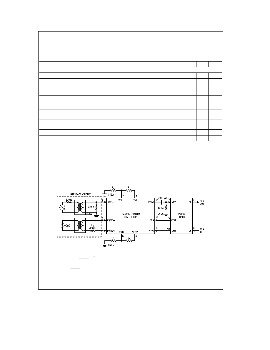
Typical Application
TL H 6660 ≠ 2
Note 1
Transmit voltage gain
e
R1
a
R2
R2
c
0
2 (The filter itself introduces a 3 dB gain) (R1
a
R2
t
10k)
Note 2
Receive gain
e
R4
R3
a
R4
(R3
a
R4
t
10k)
Note
In the configuration shown the receive filter power amplifiers will drive a 600X T to R termination to a maximum signal level of 8 5 dBm An alternative
arrangement using a transformer winding ratio equivalent to 1 414 1 and 300X resistor R
S
will provide a maximum signal level of 10 1 dBm across a 600X
termination impedance
FIGURE 2
5