 | –≠–ª–µ–∫—Ç—Ä–æ–Ω–Ω—ã–π –∫–æ–º–ø–æ–Ω–µ–Ω—Ç: uA9636A | –°–∫–∞—á–∞—Ç—å:  PDF PDF  ZIP ZIP |
DS9636A
RS-423 Dual Programmable Slew Rate Line Driver
General Description
The DS9636A is a TTL/CMOS compatible, dual, single
ended line driver which has been specifically designed to
satisfy the requirements of EIA Standard RS-423.
The DS9636A is suitable for use in digital data transmission
systems where signal wave shaping is desired. The output
slew rates are jointly controlled by a single external resistor
connected between the wave shaping control lead (WS) and
ground. This eliminates any need for external filtering of the
output signals. Output voltage levels and slew rates are in-
dependent of power supply variations. Current-limiting is
provided in both output states. The DS9636A is designed for
nominal power supplies of
±
12V.
Inputs are TTL compatible with input current loading low
enough (1/10 UL) to be also compatible with CMOS logic.
Clamp diodes are provided on the inputs to limit transients
below ground.
Features
n
Programmable slew rate limiting
n
Meets EIA Standard RS-423
n
Commercial or extended temperature range
n
Output short circuit protection
n
TTL and CMOS compatible inputs
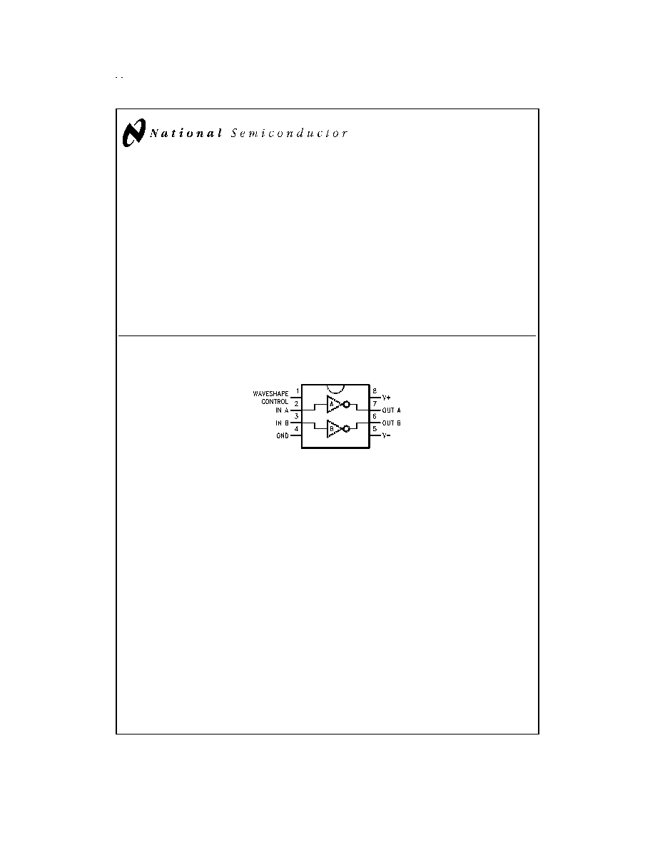
Connection Diagram
8-Lead DIP
DS009620-1
Top View
Order Number DS9636ACN,
See NS Package Number N08E
For Complete Military Product Specifications,
refer to the appropriate SMD or MDS.
Order Number DS9636AJ/883
See NS Package Number J08A
May 1998
DS9636A
RS-423
Dual
Programmable
Slew
Rate
Line
Driver
© 1998 National Semiconductor Corporation
DS009620
www.national.com
Absolute Maximum Ratings
(Note 1)
If Military/Aerospace specified devices are required,
please contact the National Semiconductor Sales Office/
Distributors for availability and specifications.
Storage Temperature Range
Ceramic DIP
-65∞C to +175∞C
Molded DIP
-65∞C to +150∞C
Lead Temperature
Ceramic DIP (Soldering, 60 seconds)
300∞C
Molded DIP (Soldering, 10 seconds)
265∞C
Maximum Power Dissipation
*
at 25∞C (Note 5)
Cavity Package
1560 mW
Molded Package
1300 mW
V+ Lead Potential to Ground Lead
V- to +15V
V- Lead Potential to Ground Lead
+0.5V to -15V
V+ Lead Potential to V- Lead
0V to +30V
Output Potential to Ground Lead
±
15V
Output Source Current
-150 mA
Output Sink Current
150 mA
Recommended Operating Conditions
Characteristics
DS9636AM
DS9636AC
Units
Min
Typ
Max
Min
Typ
Max
Positive Supply Voltage (V+)
10.8
12
13.2
10.8
12
13.2
V
Negative Supply Voltage (V-)
-13.2
-12
-10.8
-13.2
-12
-10.8
V
Operating Temperature (T
A
)
-55
25
125
0
25
70
∞C
Wave Shaping Resistance (R
WS
)
10
500
10
1000
k
Electrical Characteristics
(Notes 2, 3)
Over recommended operating temperature, supply voltage and wave shaping resistance ranges unless otherwise specified
Symbol
Parameter
Conditions
Min
Typ
Max
Units
V
OH1
Output Voltage HIGH
R
L
to GND (R
L
=
)
5.0
5.6
6.0
V
V
OH2
R
L
to GND (R
L
= 3.0 k
)
5.0
5.6
6.0
V
V
OH3
R
L
to GND (R
L
= 450
)
4.0
5.5
6.0
V
V
OL1
Output Voltage LOW
R
L
to GND (R
L
=
)
-6.0
-5.7
-5.0
V
V
OL2
R
L
to GND (R
L
= 3.0 k
)
-6.0
-5.6
-5.0
V
V
OL3
R
L
to GND (R
L
= 450
)
-6.0
-5.4
-4.0
V
R
O
Output Resistance
450
R
L
25
50
I
OS+
Output Short Circuit Current (Note 4)
V
O
= 0V, V
I
= 0V
-150
-60
-15
mA
I
OS-
V
O
= 0V, V
I
= 2.0V
15
60
150
mA
I
CEX
Output Leakage Current
V
O
=
±
6.0V, Power-Off
-100
+100
µA
V
IH
Input Voltage HIGH
2.0
V
V
IL
Input Voltage LOW
0.8
V
V
IC
Input Clamp Diode Voltage
I
I
= 15 mA
-1.5
-1.1
V
I
IL
Input Current LOW
V
I
= 0.4V
-80
-16
V
I
IH
Input Current HIGH
V
I
= 2.4V
1.0
10
µA
V
I
= 5.5V
10
100
I+
Positive Supply Current
V
CC
=
±
12V, R
L
=
,
13
18
mA
R
WS
= 100 k
, V
I
= 0V
I-
Negative Supply Current
V
CC
=
±
12V, R
L
=
,
-18
-13
mA
R
WS
= 100 k
, V
I
= 0V
Note 1: "Absolute Maximum Ratings" are those values beyond which the safety of the device cannot be guaranteed. They are not meant to imply that the devices
should be operated at these limits. The tables of "Electrical Characteristics" provide conditions for actual device operation.
Note 2: Unless otherwise specified Min/Max limits apply across the -55∞C to +125∞C temperature range for the DS9636AM and across the 0∞C to +70∞C range for
the DS9636AC. All typicals are given for V
CC
= 5V and T
A
= 25∞C.
Note 3: All currents into the device pins are positive; all currents out of the device pins are negative. All voltages are reference to ground unless otherwise specified.
Note 4: Only one output at a time should be shorted.
Note 5: Ratings apply to ambient temperature at 25∞C. Above this temperature, derate J and N packages 10.4 mW/∞C.
www.national.com
2
Switching Characteristics
V
CC
=
±
12V
±
10%, T
A
= 25∞C, see AC Test Circuit
Symbol
Parameter
Condition
Min
Typ
Max
Units
t
r
Rise Time
R
WS
= 10 k
0.8
1.1
1.4
R
WS
= 100 k
8.0
11
14
µs
R
WS
= 500 k
40
55
70
R
WS
= 1000 k
80
110
140
t
f
Fall Time
R
WS
= 10 k
0.8
1.1
1.4
R
WS
= 100 k
8.0
11
14
µs
R
WS
= 500 k
40
55
70
R
WS
= 1000 k
80
110
140
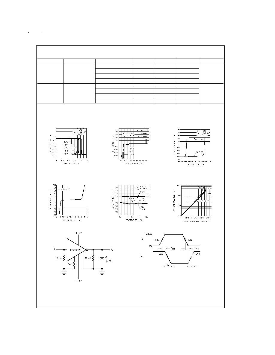
Typical Performance Characteristics
Input/Output Transfer
Characteristic vs Temperature
DS009620-7
Input Current vs
Input Voltage
DS009620-8
Output Current vs
Output Voltage (Power On)
DS009620-9
Output Current vs
Output Voltage (Power Off)
DS009620-10
Supply Current
vs Temperature
DS009620-11
Transition Time vs R
WS
DS009620-12
DS009620-4
C
L
includes jig and probe capacitance
DS009620-5
V
I
Amplitude: 3.0V
Offset: 0V
Pulse Width: 500 µs
PRR: 1.0 kHz
t
r
= t
f
10 ns
FIGURE 1. AC Test Circuit and Waveforms
www.national.com
3
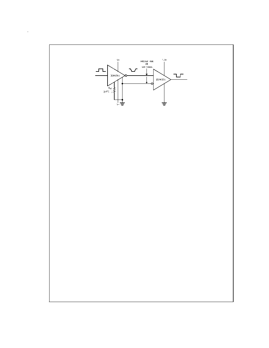
Typical Performance Characteristics
(Continued)
DS009620-6
FIGURE 2. RS-423 System Application
www.national.com
4
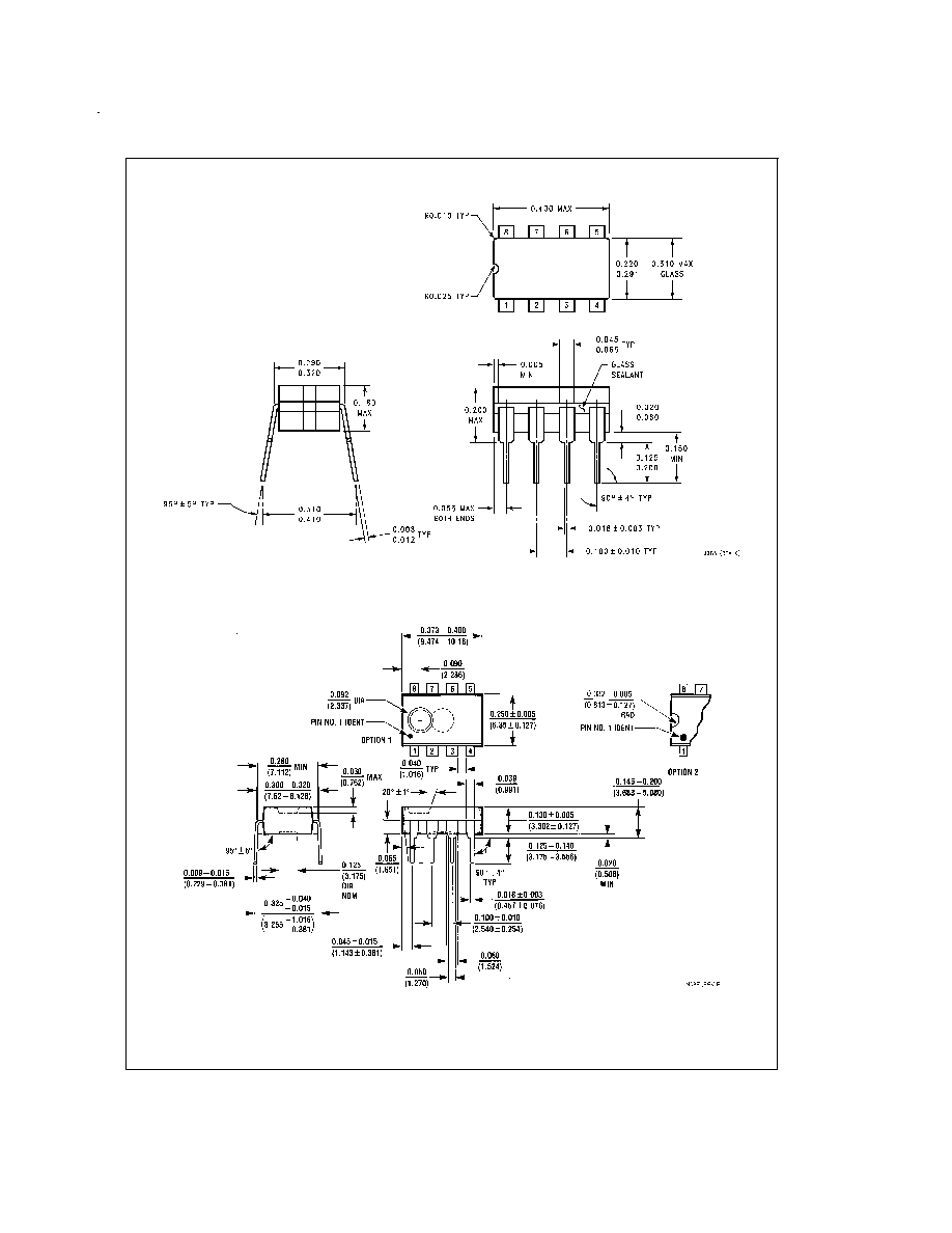
Physical Dimensions
inches (millimeters) unless otherwise noted
Ceramic Dual-In-Line Package (J)
Order Number DS9636AJ/883
NS Package Number J08A
Molded Dual-In-Line Package (N)
Order Number DS9636ACN
NS Package Number N08E
www.national.com
5
LIFE SUPPORT POLICY
NATIONAL'S PRODUCTS ARE NOT AUTHORIZED FOR USE AS CRITICAL COMPONENTS IN LIFE SUPPORT DE-
VICES OR SYSTEMS WITHOUT THE EXPRESS WRITTEN APPROVAL OF THE PRESIDENT OF NATIONAL SEMI-
CONDUCTOR CORPORATION. As used herein:
1. Life support devices or systems are devices or sys-
tems which, (a) are intended for surgical implant into
the body, or (b) support or sustain life, and whose fail-
ure to perform when properly used in accordance
with instructions for use provided in the labeling, can
be reasonably expected to result in a significant injury
to the user.
2. A critical component in any component of a life support
device or system whose failure to perform can be rea-
sonably expected to cause the failure of the life support
device or system, or to affect its safety or effectiveness.
National Semiconductor
Corporation
Americas
Tel: 1-800-272-9959
Fax: 1-800-737-7018
Email: support@nsc.com
www.national.com
National Semiconductor
Europe
Fax: +49 (0) 1 80-530 85 86
Email: europe.support@nsc.com
Deutsch Tel: +49 (0) 1 80-530 85 85
English
Tel: +49 (0) 1 80-532 78 32
FranÁais Tel: +49 (0) 1 80-532 93 58
Italiano
Tel: +49 (0) 1 80-534 16 80
National Semiconductor
Asia Pacific Customer
Response Group
Tel: 65-2544466
Fax: 65-2504466
Email: sea.support@nsc.com
National Semiconductor
Japan Ltd.
Tel: 81-3-5620-6175
Fax: 81-3-5620-6179
DS9636A
RS-423
Dual
Programmable
Slew
Rate
Line
Driver
National does not assume any responsibility for use of any circuitry described, no circuit patent licenses are implied and National reserves the right at any time without notice to change said circuitry and specifications.