NTE1171
Integrated Circuit
Operational Amplifier
Description:
The NTE1171 is a general purpose operational amplifier in an 8≠Lead Metal Can type package. Ad-
vanced processing techniques make possible an order of magnitude reduction in input currents, and
a redesign of the biasing circuitry reduces the temperature drift of the input current.
This amplifier offers many features which make its application nearly foolproof: overload protection
on the input, no latch≠up when the common mode range is exceeded, freedom from oscillations and
compensations with a single 30pF capacitor. It has advantages over internally compensated amplifi-
ers in that the frequency compensation can be tailored to the particular application. For example, in
low frequency circuits it can be overcompensated for increased stability margin. Or the compensation
can be optimized to give more than a factor of ten improvement in high frequency performance for
most applications.
Feature:
D
Low Input Offset Current: 20na Maximum Over Temperature Range
D
External Frequency Compensation for Flexibility
D
Class AB Output Provides Excellent Linearity
D
Output Short≠Circuit Protection
D
Guaranteed Drift Characteristics
Absolute Maximum Ratings:
Power Supply Voltage, V
CC
, V
EE
±
18V
. . . . . . . . . . . . . . . . . . . . . . . . . . . . . . . . . . . . . . . . . . . . . . . . . . . .
Input Differential Voltage, V
ID
±
30V
. . . . . . . . . . . . . . . . . . . . . . . . . . . . . . . . . . . . . . . . . . . . . . . . . . . . . . .
Input Common≠Mode Range (Note 1), V
ICR
±
15V
. . . . . . . . . . . . . . . . . . . . . . . . . . . . . . . . . . . . . . . . . .
Output Short≠Circuit Duration, t
S
Continuous
. . . . . . . . . . . . . . . . . . . . . . . . . . . . . . . . . . . . . . . . . . . . . .
Power Dissipation (Package Limitation, T
A
= +25
∞
C), P
D
500mW
. . . . . . . . . . . . . . . . . . . . . . . . . . . .
Derate Above T
A
= +75
∞
C
6.8mW/
∞
C
. . . . . . . . . . . . . . . . . . . . . . . . . . . . . . . . . . . . . . . . . . . . . . .
Operating Ambient Temperature Range, T
A
0
∞
to +70
∞
C
. . . . . . . . . . . . . . . . . . . . . . . . . . . . . . . . . . . . .
Storage Temperature Range, T
stg
≠65
∞
to +150
∞
C
. . . . . . . . . . . . . . . . . . . . . . . . . . . . . . . . . . . . . . . . . .
Note 1. For supply voltages less than
±
15V, the avbsolute maximum input voltage is equal to the supply
voltage.
Electrical Characteristics: (T
A
= +25
∞
C, V
CC
=
±
5V to
±
15V unless otherwise specified)
Parameter
Symbol
Test Conditions
Min
Typ
Max
Unit
Input Offset Voltage
V
IO
R
S
50k
≠
2.0
7.5
mV
Input Offset Current
I
IO
≠
3.0
50
nA
Input Bias Current
I
IB
≠
70
250
nA
Input Resistance
r
i
0.5
2.0
≠
M
Supply Current
I
CC
, I
EE
V
CC
/V
EE
=
±
15V
≠
1.8
3.0
mA
Large Signal Voltage Gain
A
V
V
CC
/V
EE
=
±
15V, V
O
=
±
10V,
R
L
> 2k
25
160
≠
V/mV
Note: The following specifications apply over the operating temperature range.
Input Offset Voltage
V
IO
R
S
50k
≠
≠
10
mV
Input Offset Current
I
IO
≠
≠
70
nA
Average Temperature Coefficient
of Input Offset Voltage
V
IO
/
T
T
A
(min)
T
A
T
A
(max)
≠
6.0
30
µ
V/
∞
C
Average Temperature Coefficient
I
IO
/
T
+25
∞
C
T
A
T
A
(max)
≠
0.01
0.3
nA/
∞
C
of Input Offset Current
T
A
(min)
T
A
+25
∞
C
≠
0.02
0.6
nA/
∞
C
Input Bias Current
I
IB
≠
≠
300
nA
Large Signal Voltage Gain
A
V
V
CC
/V
EE
=
±
15V, V
O
=
±
10V,
R
L
> 2k
15
≠
≠
V/mV
Input Voltage Range
V
I
V
CC
/V
EE
=
±
15V
±
12
≠
≠
V
Common≠Mode Rejection Ratio
CMRR
R
S
50k
70
90
≠
dB
Supply Voltage Rejection Ratio
PSRR
R
S
50k
70
96
≠
dB
Output Voltage Swing
V
O
V
CC
/V
EE
=
±
15V, R
L
= 10k
±
12
±
14
≠
V
V
CC
/V
EE
=
±
15V, R
L
= 2k
±
10
±
13
≠
V
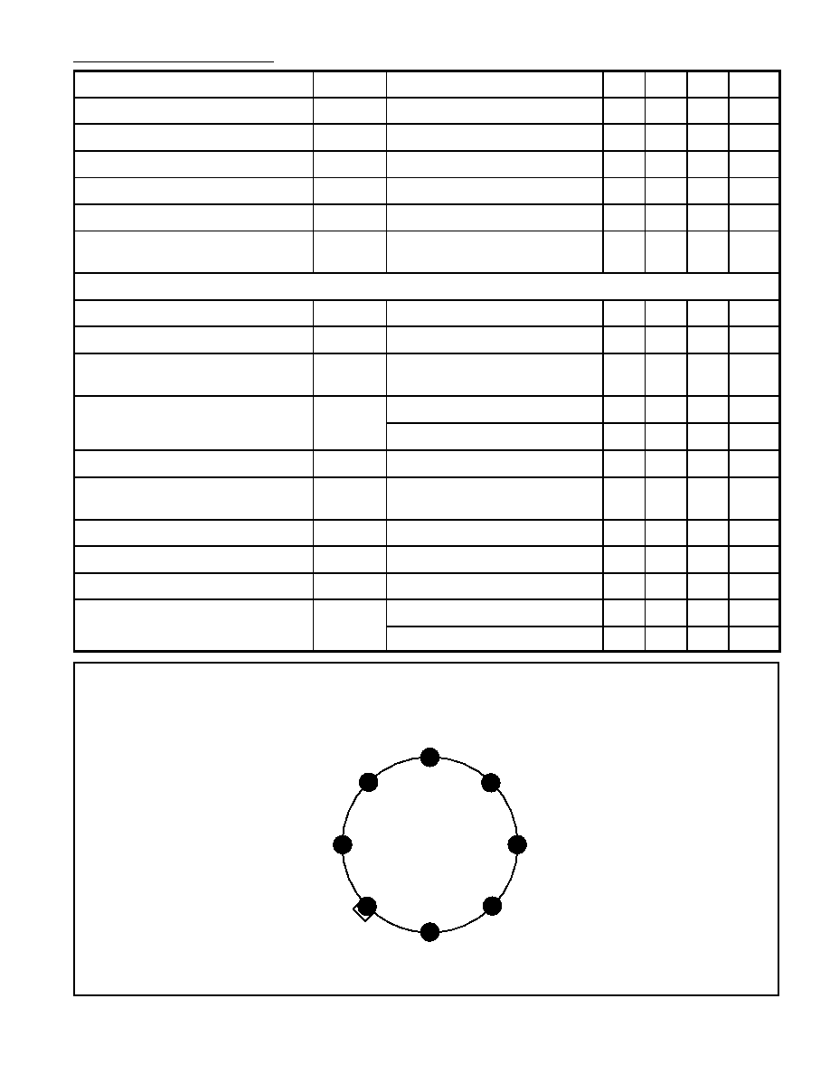
Pin Connection Diagram
(Top View)
8
7
6
5
4
3
2
1
Phase Compensation
Inverting Input
Non≠Inverting Input
V (≠)
Offset Null
Output
V (+)
Phase Compensation