
NTE1177
Integrated Circuit
TV Luminance Processor
Description:
The NTE1177 is a monolithic silicon integrated circuit in a 14≠Lead DIP type package that performs
the luminance processing functions of amplification; contrast, brightness and peaking control; blank-
ing; and black≠level clamping.
Features:
D
Black≠Level Clamping
D
Linear DC Controls for Brightness, Contrast, and Peaking
D
Horizontal and Vertical Blanking
D
Operates with Standard or Tapped Delay Line
Absolute Maximum Ratings;
DC Supply Current (Into Pin13, Note 1), V
CC
59.5mA
. . . . . . . . . . . . . . . . . . . . . . . . . . . . . . . . . . . . . . .
Device Dissipation (Up to T
A
= +55
∞
C, Note 1), P
D
750mW
. . . . . . . . . . . . . . . . . . . . . . . . . . . . . . . . . .
Derate Above 55
∞
C 7.9mW/
∞
C
. . . . . . . . . . . . . . . . . . . . . . . . . . . . . . . . . . . . . . . . . . . . . . . . . . . .
Operating Ambient Temperature Range, T
opr
≠40
∞
to +85
∞
C
. . . . . . . . . . . . . . . . . . . . . . . . . . . . . . . . . .
Storage Temperature Range, T
stg
≠65
∞
to +150
∞
C
. . . . . . . . . . . . . . . . . . . . . . . . . . . . . . . . . . . . . . . . . .
Lead Temperature (During Soldering, 1/16" from case, 10sec max), T
L
+265
∞
C
. . . . . . . . . . . . . . . . .
Note 1. Although the NTE1177 is rated for maximum dissipation of 750mW, it is recommended that
the current into Pin13 be limited by external circuit resistance to 39mA for a typical voltage
at Pin13 of 11.8V.
Electrical Characteristics: (T
A
= +25
∞
C unless otherwise specified)
Test Conditions
Switch Numbers
S1
S2
S3
S4
S5
S6
S7
S8
S9 S10 S11
Parameter
Symbol
Switch Positions
For Characteristic Measurements
Min
Typ
Max
Unit
Static Characteristics (Bias Voltage = 6.1V)
Voltage at Pin13
V
13
2
1
1
2
2
4
1
2
2
1
1
11.0
11.8
13.2
V
Quiescent Voltage
V
4
2
1
1
2
2
3
1
2
2
1
1
3.3
4.0
5.7
V
V
7
2
1
1
2
2
2
1
2
2
1
1
7.1
7.7
8.3
V
Current Into Pin13
Pin13 Connected
to +11V
I
13
2
1
1
2
2
3
1
2
2
1
2
10
19
30
mA
Electrical Characteristics (Cont'd): (T
A
= +25
∞
C unless otherwise specified)
Test Conditions
Switch Numbers
S1
S2
S3
S4
S5
S6
S7
S8
S9 S10 S11
Parameter
Switch Positions
For Characteristic Measurements
Min
Typ
Max
Unit
Dynamic Characteristics (Bias Voltage = 5.8V)
Wide≠Band Gain (Note 2)
1
1
1
2
1
2
1
1
1
2
1
6.0
8.3
11.0
dB
Contrast Gain Reduction (Note 3)
1
1
1
2
1
2
1
1
2
2
1
27
30
≠
dB
Peaking Gain (Note 2)
1
1
2
2
1
2
1
1
1
2
1
15.0
18.4
22.0
dB
Peaking Gain Reduction (Note 4)
1
1
2
2
1
2
1
1
1
2
1
16
18
≠
dB
Max. Intermodulation Distortion
2V (Note 5)
1
≠
1
1
1
2
≠
2
1
2
1
≠
20
≠
%
3V (Note 6)
1
≠
1
1
1
2
≠
2
1
2
1
≠
40
≠
%
Note 2. Set 50kHz generator for 100mV
P≠P
Adjust R1 Peaking Control for minimum setting. Measure
wide≠band gain at Pin7.
Note 3. Set 50kHz generator for 100mV
P≠P
. Adjust R1 for minimum setting. Measure contrast gain
reduction at Pin7.
Note 4. Set 50kHz generator for 100mV
P≠P
. Adjust R1 for maximum setting. Measure peaking gain
reduction at Pin7.
Note 5. Adjust R1 for minimum setting. With S2 at switch position 1 and S7 at switch position 3, set
50kHz generator for 2V
P≠P
. Then with S2 at switch position 2, set 1MHz generator for
100mV
P≠P
. Then with S7 at switch position 2, measure downward modulation of the 1MHz
signal due to the 50kHz signal.
Note 6. Repeat step 5 except that the 50kHz generator must be set at 3V
P≠P
.
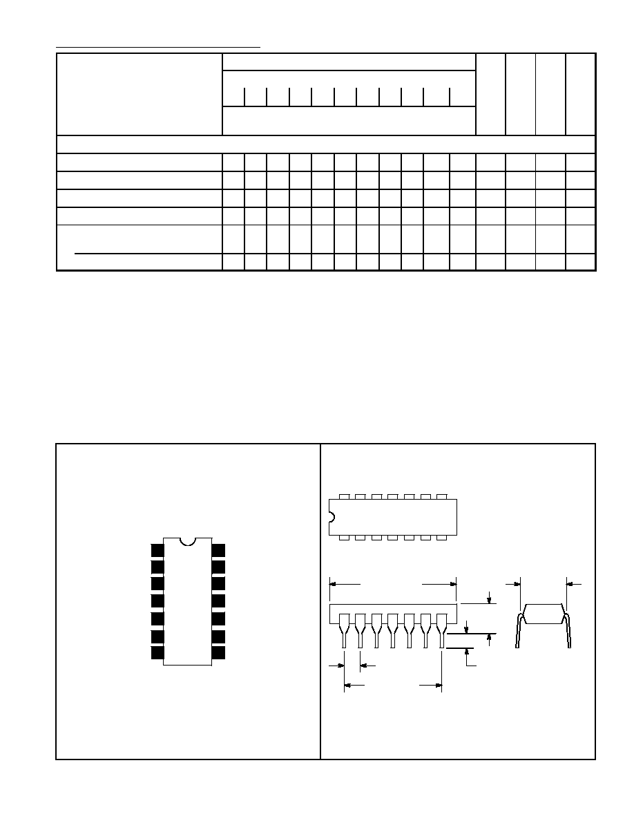
.600 (15.24)
1
7
14
8
.300
(7.62)
.200 (5.08)
Max
.100 (2.45)
.099 (2.5) Min
.785 (19.95)
Max
Pin Connection Diagram
Blanking Input
Clamp Inhibit Input
Contrast Control
Video Input
N.C.
Peaking Control
Video Output
Peaking Input
Brightness Control
Shunt Regulator
Clamped Video Out
Clamp Inhibit
Substrate GND
Peaking Input
1
2
3
4
5
6
7
14
13
12
11
10
9
8
and Bypass