NTE1232
Integrated Circuit
Audio Amplifier for Car Radio, 8W
Description:
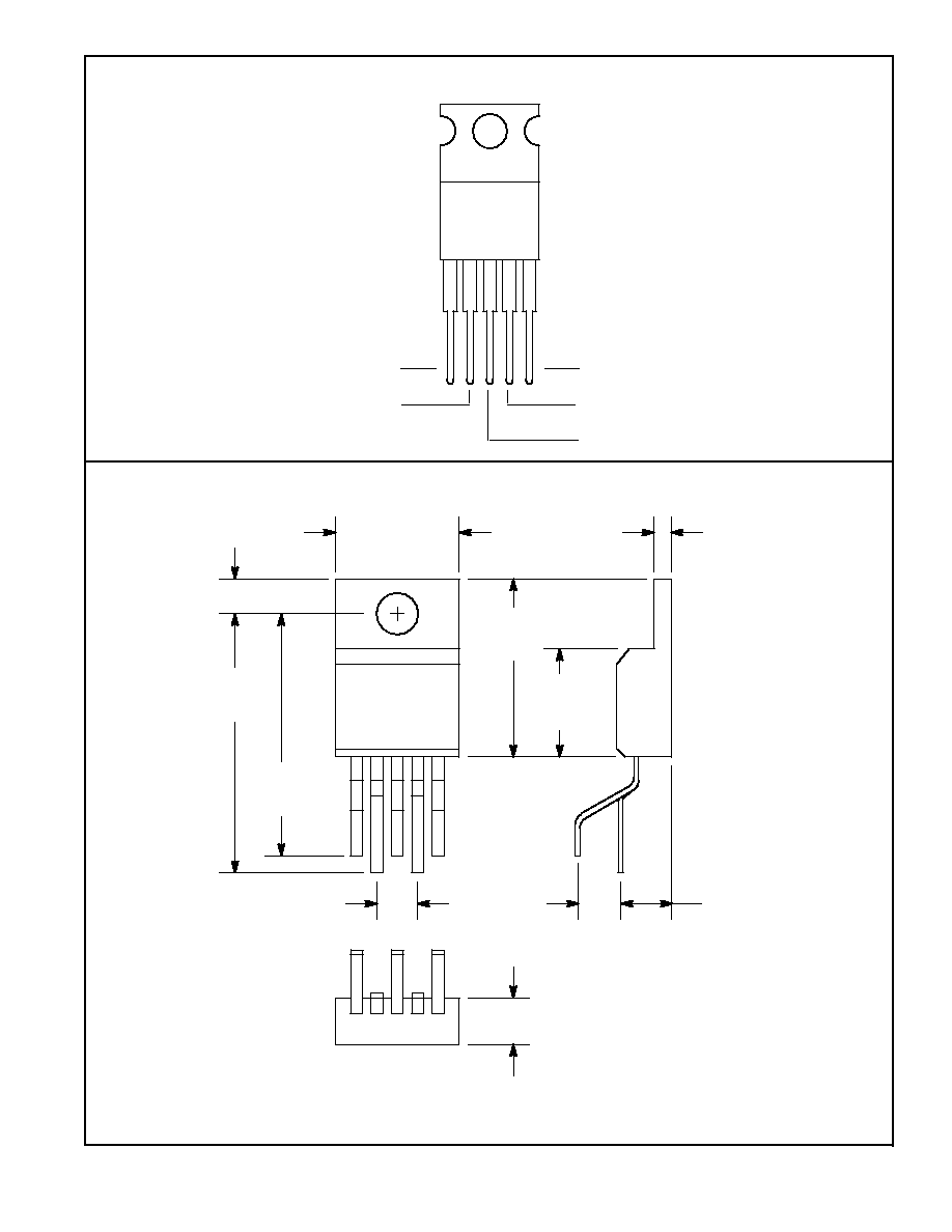
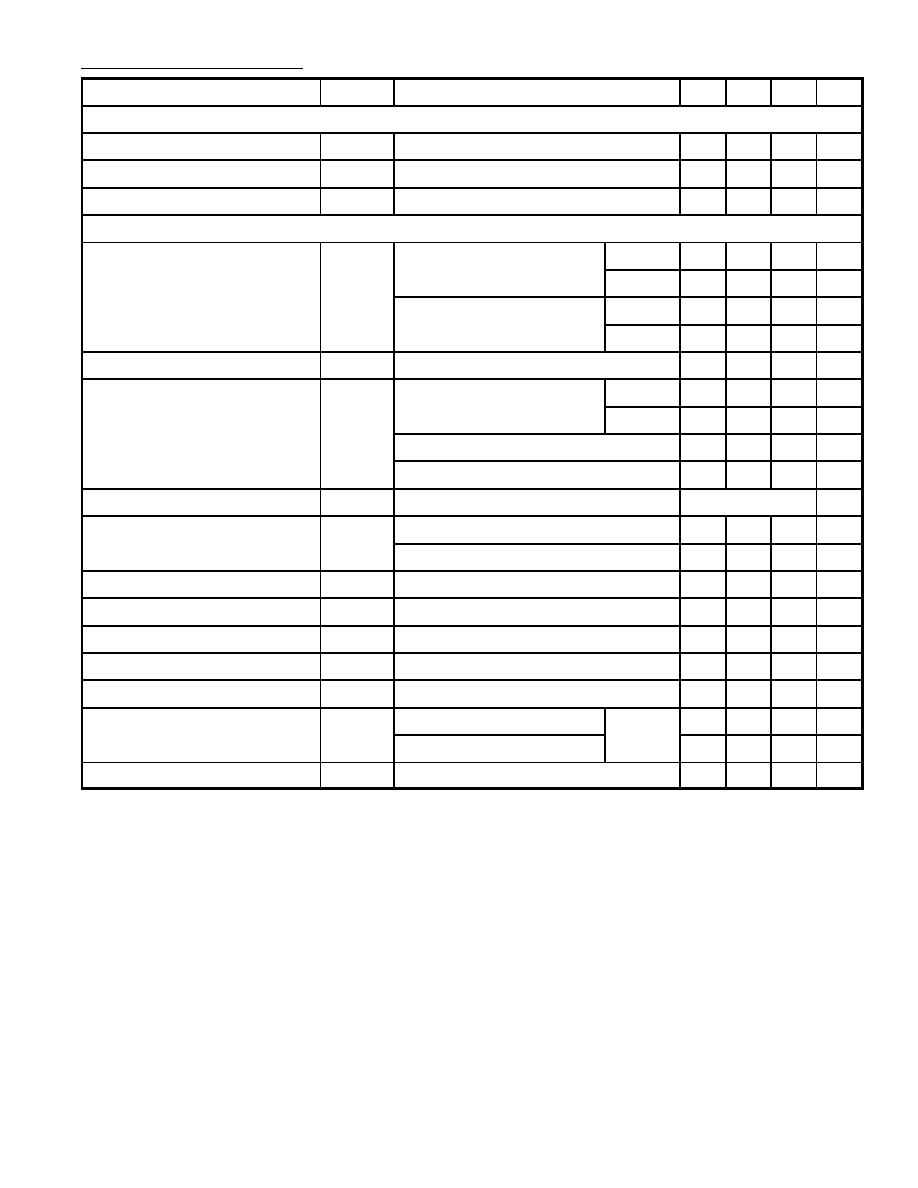
The NTE1232 is a Class B audio amplifier in a 5≠Lead TO220 type package designed for driving low
impedance loads (down to 1.6
). This device provides a high output current capability (up to 3.5A),
very low harmonic and cross≠over distortion.
Features:
D
Low Number of External Components
D
No Electrical Insulation Requirement
D
Space and Cost Saving
D
High Reliability
D
Flexibility in Use
D
Complete Safety During Operation due to Protection Against:
Short Circuit
Thermal Over Range
Fortuitous Open Ground
Polarity Inversion (V
s
= 12V Max)
Load Dump Voltage Surge
Absolute Maximum Ratings;
Peak Supply Voltage (50ms), V
s
40V
. . . . . . . . . . . . . . . . . . . . . . . . . . . . . . . . . . . . . . . . . . . . . . . . . . . . . .
DC Supply Voltage, V
s
28V
. . . . . . . . . . . . . . . . . . . . . . . . . . . . . . . . . . . . . . . . . . . . . . . . . . . . . . . . . . . . . .
Operating Supply Voltage, V
s
18V
. . . . . . . . . . . . . . . . . . . . . . . . . . . . . . . . . . . . . . . . . . . . . . . . . . . . . . . .
Output Peak Current, I
o
Repetitive
3.5A
. . . . . . . . . . . . . . . . . . . . . . . . . . . . . . . . . . . . . . . . . . . . . . . . . . . . . . . . . . . . . . . . . .
Non≠Repetitive
4.5A
. . . . . . . . . . . . . . . . . . . . . . . . . . . . . . . . . . . . . . . . . . . . . . . . . . . . . . . . . . . . .
Power Dissipation (T
C
= +90
∞
C), P
tot
15W
. . . . . . . . . . . . . . . . . . . . . . . . . . . . . . . . . . . . . . . . . . . . . . . . .
Operating Junction Temperature Range, T
J
≠40
∞
to +150
∞
C
. . . . . . . . . . . . . . . . . . . . . . . . . . . . . . . . . .
Storage Temperature Range, T
stg
≠40
∞
to +150
∞
C
. . . . . . . . . . . . . . . . . . . . . . . . . . . . . . . . . . . . . . . . . .
Thermal Resistance, Junction≠to≠Case, R
thJC
4
∞
C/W max
. . . . . . . . . . . . . . . . . . . . . . . . . . . . . . . . . .
Electrical Characteristics: (V
S
= 14.4V, T
A
= +25
∞
C unless otherwise specified)
Parameter
Symbol
Test Conditions
Min
Typ Max Unit
DC Characteristics
Supply Voltage
V
s
8
≠
18
V
Quiescent Output Voltage (Pin4)
V
o
6.4
7.2
8.0
V
Quiescent Drain Current (Pin5)
I
d
≠
45
80
mA
AC Characteristics (G
V
= 40dB)
Output Power
P
o
d = 10%, f = 1kHz
R
L
= 4
4.8
5.2
≠
W
R
L
= 2
7.0
8.0
≠
W
V
s
= 16V, d = 10%, f = 1kHz R
L
= 4
≠
6.5
≠
W
R
L
= 2
≠
10
≠
W
Input Saturation Voltage
V
i(rms)
600
≠
≠
mV
Input Sensitivity
V
i
f = 1kHz, P
o
= 0.5W
R
L
= 4
≠
15
≠
mV
R
L
= 2
≠
11
≠
mV
f = 1kHz, P
o
= 5.2W, R
L
= 4
≠
55
≠
mV
f = 1kHz, P
o
= 8W, R
L
= 2
≠
50
≠
mV
Frequency Response (≠3dB)
B
R
L
= 4
, P
o
= 1W
40 to 15,000
Hz
Distortion
d
f = 1kHz, P
o
= 0.05 to 3.5W, R
L
= 4
≠
0.2
≠
%
f = 1kHz, P
o
= 0.05 to 5W, R
L
= 2
≠
0.2
≠
%
Input Resistance (Pin1)
R
i
f = 1kHz
70
150
≠
k
Voltage Gain (Open Loop)
G
V
f = 1kHz, R
L
= 4
≠
80
≠
dB
Voltage Gain (Closed Loop)
G
V
f = 1kHz, R
L
= 4
39.5 40.0 40.5
dB
Input Noise Voltage
e
N
Note 1
≠
4
≠
µ
V
Input Noise Current
i
N
Note 1
≠
60
≠
pA
Efficiency
P
o
= 5.2W, R
L
= 4
f = 1kHz
≠
68
≠
%
P
o
= 8W, R
L
= 2
≠
58
≠
%
Supply Voltage Rejection
SVR
R
L
= 4
, R
g
= 10k
, f
ripple
= 100Hz
30
35
≠
dB
Note 1. Filter with noise bandwidth: 22Hz to 22kHz.