NTE1292
Integrated Circuit
IF Amplifier and Detector
Description:
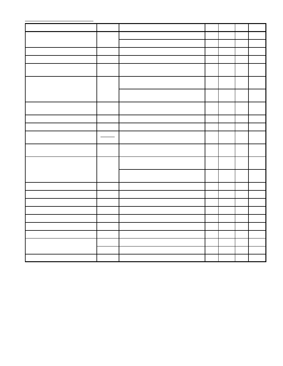
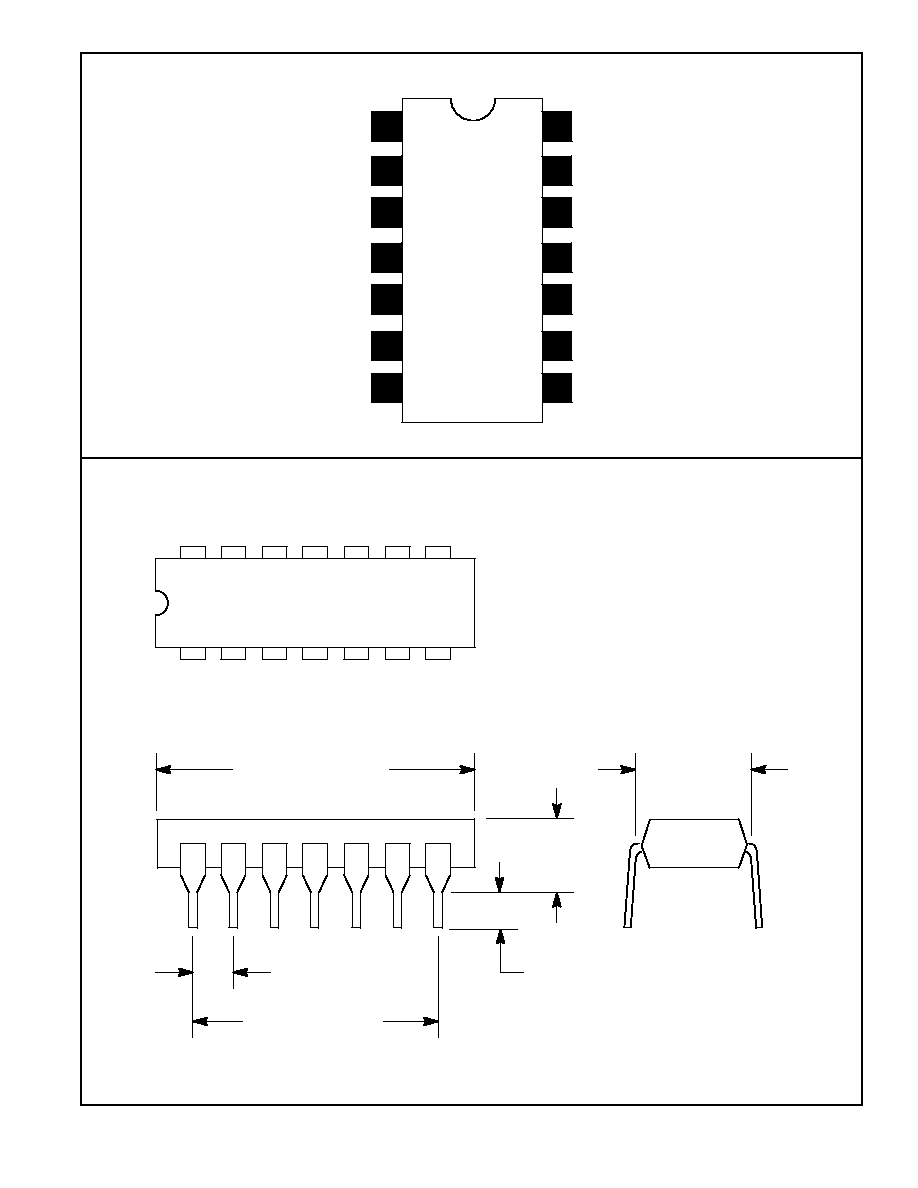
The NTE1292 is a monolithic integrated circuit in a 14≠Lead DIP type package specifically designed
for audio detection in TV and FM radio receivers. It incorporates an 8≠stage limiting IF amplifier and
balanced detector plus a DC operated volume control.
Pin3 and Pin4 are connected to the collector and base of a transistor which may be used as an AF≠
preamplifier or as a switch.
At Pin12 a zener≠diode is accessible which can be used to stabilize the supply voltage of this inte-
grated circuit or the voltage of other circuit elements in the set.
Features:
D
Electronic Attenuator: Replaces Conventional AC Volume Control
D
Volume Reduction Range: 85dB Typ
D
Sensitivity: 3dB Limiting Voltage 30
µ
V Typ
D
Excellent AM Rejection 68dB Typ at 10mV
D
Audio Output Voltage: 1V Typ
D
Wide Supply Voltage Range: V
CC
= 6V to 18V
D
Internal Zener Diode Regulator
D
Very Low External Component Requirement
D
Simple Detector Alignment: One Coil
Absolute Maximum Ratings:
Supply Voltage, V
11
18V
. . . . . . . . . . . . . . . . . . . . . . . . . . . . . . . . . . . . . . . . . . . . . . . . . . . . . . . . . . . . . . . . .
Volume Control Voltage, V
5
4V
. . . . . . . . . . . . . . . . . . . . . . . . . . . . . . . . . . . . . . . . . . . . . . . . . . . . . . . . . . .
Zener Current, I
12
20mA
. . . . . . . . . . . . . . . . . . . . . . . . . . . . . . . . . . . . . . . . . . . . . . . . . . . . . . . . . . . . . . . .
Transistor Collector Current, I
3
5mA
. . . . . . . . . . . . . . . . . . . . . . . . . . . . . . . . . . . . . . . . . . . . . . . . . . . . . .
Transistor Base Current, I
4
2mA
. . . . . . . . . . . . . . . . . . . . . . . . . . . . . . . . . . . . . . . . . . . . . . . . . . . . . . . . .
Bias Resistance (Max), R
13≠14
1k
. . . . . . . . . . . . . . . . . . . . . . . . . . . . . . . . . . . . . . . . . . . . . . . . . . . . . . .
Operating Temperature Range, T
opr
≠15
∞
to +70
∞
C
. . . . . . . . . . . . . . . . . . . . . . . . . . . . . . . . . . . . . . . . .
Storage Temperature Range, T
stg
≠65
∞
to +150
∞
C
. . . . . . . . . . . . . . . . . . . . . . . . . . . . . . . . . . . . . . . . . .