NTE1293
Integrated Circuit
Dual, Audio Power Amp, 5.8W/Ch
Description:
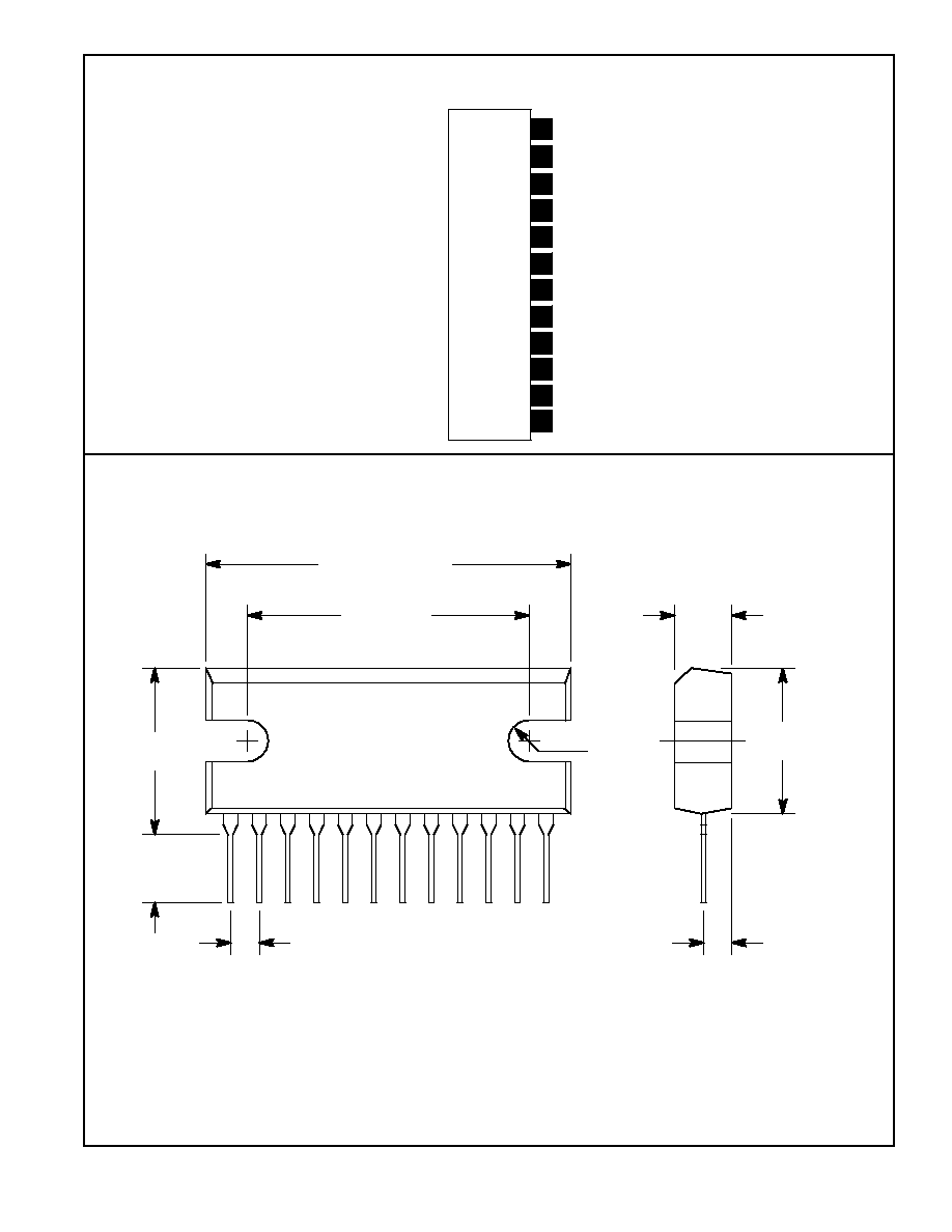
The NTE1293 is a dual audio power amplifier in a 12≠Lead SIP type package specifically designed
for car stereo applications. This device provides an output power of 7W/Ch to a 4
load with 10%
THD at 14.4V power supply.
Features:
D
Very Low Number of External Components Required
D
Easy Mounting with No Electrical Isolation Between the Package and Heat Sink
D
Very Low Transient Noise at Power Switch≠On
D
No Damage for Reverse Insertion on the PC Board
D
Thermal Shut≠Down Circuit Included
D
Load Dump Protection Circuit Included
Absolute Maximum Ratings: (T
A
= +25
∞
C unless otherwise specified)
Supply Voltage (Surge PW = 200ms), V
CC
surge
40V
. . . . . . . . . . . . . . . . . . . . . . . . . . . . . . . . . . . . . . . .
Supply Voltage (Quiescent, Note 1), V
CC1
25V
. . . . . . . . . . . . . . . . . . . . . . . . . . . . . . . . . . . . . . . . . . . . .
Supply Voltage (Operational), V
CC2
18V
. . . . . . . . . . . . . . . . . . . . . . . . . . . . . . . . . . . . . . . . . . . . . . . . . . .
Peak Circuit Current, I
CC
peak
4.5A
. . . . . . . . . . . . . . . . . . . . . . . . . . . . . . . . . . . . . . . . . . . . . . . . . . . . . . .
package Dissipation, P
D
20W
. . . . . . . . . . . . . . . . . . . . . . . . . . . . . . . . . . . . . . . . . . . . . . . . . . . . . . . . . . . .
Operating Temperature Range (Note 1), T
opr
≠30
∞
to +75
∞
C
. . . . . . . . . . . . . . . . . . . . . . . . . . . . . . . . . .
Storage Temperature Range, T
stg
≠55
∞
to +150
∞
C
. . . . . . . . . . . . . . . . . . . . . . . . . . . . . . . . . . . . . . . . . .
Note 1. Using an aluminum heat sink, R
thCA
= 6
∞
C/W.
Electrical Characteristics: (T
A
= +25
∞
C, V
CC
= 13.2V, f = 1kHz, R
L
= 4
unless otherwise specified)
Parameter
Symbol
Test Conditions
Min
Typ
Max
Unit
Circuit Current
I
CC
v
in
= 0
30
80
180
mA
Output Power
P
O
THD = 10%, V
CC
= 14.4V
≠
7.0
≠
W
THD = 10%, V
CC
= 13.2V
5.0
5.8
≠
W
THD = 10%, V
CC
= 14.4V, R
L
= 2
≠
8.5
≠
W
Total Harmonic Distortion
THD
P
O
= 0.5W
≠
0.3
1.0
%
P
O
= 2W, R
L
= 2
≠
0.4
≠
%
Voltage Gain
A
V
P
O
= 0.5W
51
54
58
dB
Channel Balance
A
V
P
O
= 0.5W
≠
≠
±
1.5
dB
Crosstalk
CT
f = 1kHz, other channel R
G
= 0
30
45
≠
dB
Output Noise Level
v
n
R
G
= 10k
≠
1.4
4.0
mV
rms