NTE1295
Integrated Circuit
TV Signal Processor
Description:
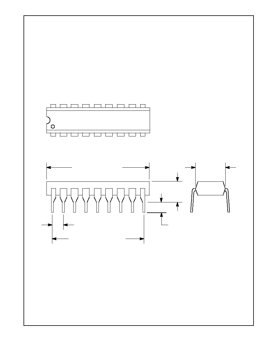
The NTE1295 is an integrated circuit in an 18≠Lead DIP type package designed for color TV deflec-
tion signal processing circuit. It can be operated with 12V power supply and is suitable for compact
and medium≠sized color TV sets.
Features:
D
Built≠In Vertical Deflection Driver Circuit
D
Incorporating Vertical and Horizontal Oscillator Circuit, Operations Highly Stable Against
Changes in Supply Voltage and Temperature.
D
Highly Stable Synchronous Separation Circuit Against Noise
D
Built≠In High Tension Protector Circuit (X≠Ray Protection)
D
12V Supply Voltage Operation.
Absolute Maximum Ratings: (T
A
= +25
∞
C, Note 1 unless otherwise specified)
Supply Voltage
V
7≠8
10.5V
. . . . . . . . . . . . . . . . . . . . . . . . . . . . . . . . . . . . . . . . . . . . . . . . . . . . . . . . . . . . . . . . . . . . . .
V
15≠8
14.4V
. . . . . . . . . . . . . . . . . . . . . . . . . . . . . . . . . . . . . . . . . . . . . . . . . . . . . . . . . . . . . . . . . . . . .
Circuit Voltage
V
1≠8
0 to 10V
. . . . . . . . . . . . . . . . . . . . . . . . . . . . . . . . . . . . . . . . . . . . . . . . . . . . . . . . . . . . . . . . . . . .
V
10≠8
0 to V
15≠8
. . . . . . . . . . . . . . . . . . . . . . . . . . . . . . . . . . . . . . . . . . . . . . . . . . . . . . . . . . . . . . . . . .
V
12≠8
0 to V
15≠8
. . . . . . . . . . . . . . . . . . . . . . . . . . . . . . . . . . . . . . . . . . . . . . . . . . . . . . . . . . . . . . . . . .
V
17≠8
≠0.6 to 6.0V
. . . . . . . . . . . . . . . . . . . . . . . . . . . . . . . . . . . . . . . . . . . . . . . . . . . . . . . . . . . . . . . .
V
18≠8
≠3 to +2V
. . . . . . . . . . . . . . . . . . . . . . . . . . . . . . . . . . . . . . . . . . . . . . . . . . . . . . . . . . . . . . . . . .
Supply Current
I
7
15mA
. . . . . . . . . . . . . . . . . . . . . . . . . . . . . . . . . . . . . . . . . . . . . . . . . . . . . . . . . . . . . . . . . . . . . . . . .
I
15
20mA
. . . . . . . . . . . . . . . . . . . . . . . . . . . . . . . . . . . . . . . . . . . . . . . . . . . . . . . . . . . . . . . . . . . . . . . .
Circuit Current
I
2
≠3 to +3mA
. . . . . . . . . . . . . . . . . . . . . . . . . . . . . . . . . . . . . . . . . . . . . . . . . . . . . . . . . . . . . . . . . . . .
I
3
≠5 to 0mA
. . . . . . . . . . . . . . . . . . . . . . . . . . . . . . . . . . . . . . . . . . . . . . . . . . . . . . . . . . . . . . . . . . . . .
I
4
≠5 to +5mA
. . . . . . . . . . . . . . . . . . . . . . . . . . . . . . . . . . . . . . . . . . . . . . . . . . . . . . . . . . . . . . . . . . . .
I
5
≠1 to +1mA
. . . . . . . . . . . . . . . . . . . . . . . . . . . . . . . . . . . . . . . . . . . . . . . . . . . . . . . . . . . . . . . . . . . .
I
6
≠20 to 0mA
. . . . . . . . . . . . . . . . . . . . . . . . . . . . . . . . . . . . . . . . . . . . . . . . . . . . . . . . . . . . . . . . . . . .
I
9
≠15 to 0mA
. . . . . . . . . . . . . . . . . . . . . . . . . . . . . . . . . . . . . . . . . . . . . . . . . . . . . . . . . . . . . . . . . . . .
I
12
≠1 to +150mA
. . . . . . . . . . . . . . . . . . . . . . . . . . . . . . . . . . . . . . . . . . . . . . . . . . . . . . . . . . . . . . . . .
I
13
0 to 40mA
. . . . . . . . . . . . . . . . . . . . . . . . . . . . . . . . . . . . . . . . . . . . . . . . . . . . . . . . . . . . . . . . . . . .
Power Dissipation, P
D
450mW
. . . . . . . . . . . . . . . . . . . . . . . . . . . . . . . . . . . . . . . . . . . . . . . . . . . . . . . . . .
Operating Ambient Temperature Range, T
opr
≠20
∞
to +70
∞
C
. . . . . . . . . . . . . . . . . . . . . . . . . . . . . . . . . .
Storage Temperature Range, T
stg
≠55
∞
to +150
∞
C
. . . . . . . . . . . . . . . . . . . . . . . . . . . . . . . . . . . . . . . . . .
Note 1.
and
are flow≠in and flow≠out currents to/from the circuit, respectively.
Electrical Characteristics: (T
A
= +25
∞
C unless otherwise specified)
Parameter
Symbol
Test Conditions
Min
Typ
Max
Unit
Circuit Current
I
7
Apply 12V with 240
to Pin7
7.5
11.2
15.0
mA
I
15
V
15≠8
= 12V
15.5
23.0
32.0
mA
Protector Operating Voltage
V
5≠8
Apply 12V with 240
to Pin7
0.64
0.70
0.76
V
Oscillation Starting Voltage
(V
O
sc
)
V
OSC≠S
f
VO
= 40 to 70Hz, 1.0V
P≠P
or More
≠
≠
6.2
V
Vertical Oscillation Frequency
f
VO
V
CC1
= 12V
53
55
58
Hz
f
VO
Change with Supply Voltage
f
VO
/V
CC
f
VO|9.6V
to f
VO|14.4V
0
0.93
1.3
Hz
Pulse Width (V
O
sc
)
t
V
CC1
= 12V
500
600
820
µ
s
Vertical Pull≠In Range
f
VP
R
OSC
= 10.93k
, (f
VO
= 48
±
1.5Hz)
≠
≠
50
Hz
Vertical Sawtooth Wave
Amplification
v
(saw)
R
SAW
= 26.4k
1.8
2.0
2.2
V
P≠P
f
VO
Change with Ambient
Temperature
f
VO
/T
A
T
A
= ≠20
∞
to +70
∞
C, Note 2
≠220
≠170
0
ppm/
∞
C
v
(saw)
Change with Ambient
Temperature
v
(saw)/T
A T
A
= ≠20
∞
to +70
∞
C, Note 2
≠
≠
30
mV
P≠P
/
∞
C
Vertical Output Tr Drive Current
I
9
≠
≠
7.5
mA
Oscillation Starting Voltage
(H
O
sc
)
V
OSC≠S
f
HO
= 10 to 20kHz,
1.4V
P≠P
or More (V
CC2
= 6.5V)
≠
≠
6
V
Horizontal Oscillation Frequency
f
HO
V
CC2
= 12V
15.0
15.6
16.25
kHz
f
HO
Change with Supply Voltage
f
HO
/V
CC
f
HO|13V
to fH
O|10V
0
25
45
Hz
Pulse Width Duty Ratio (H
O
sc
)
t
V
CC2
= 12V
32.0
36.0
39.5
%
f
HO
Control Sensitivity
b
I
O
=
±
100mA
19
21
23
Hz/
µ
A
f
HO
Change with Ambient
Temperature
f
HO
/T
A
T
A
= ≠20
∞
to +70
∞
C, Note 2
≠210
≠100
0
ppm/
∞
C
AFC Loop Gain
f
AFC
m
x
b
5800
7700
9600
Hz/rad
Note 2. Design reference value.
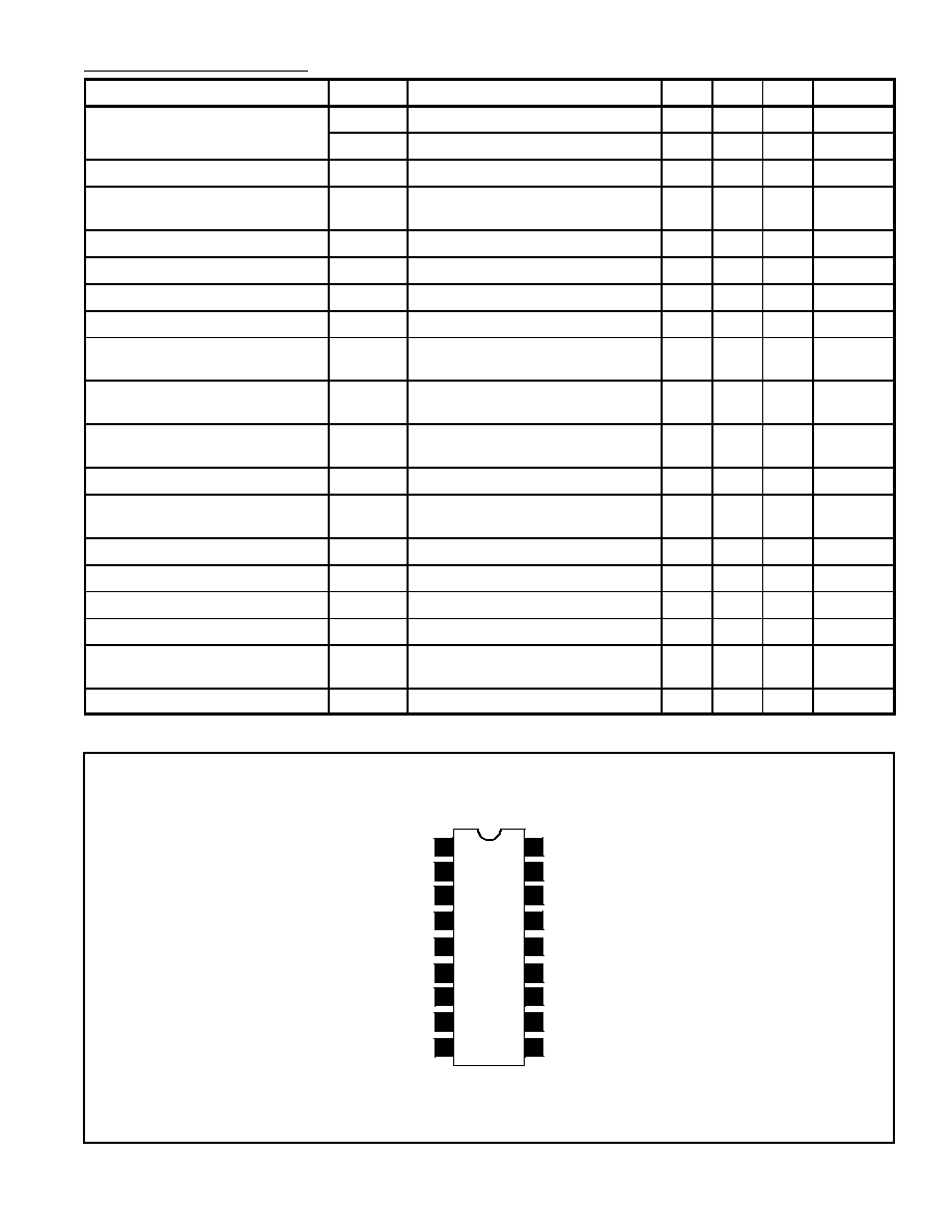
V
CC
Vert Output
Vert Height
Vert Ramp Generator
1
2
3
4
Horiz Sawtooth
Filter
Horiz Hold
Bypass
5
Protector Input
6
Horiz Driver
7
Voltage Regulator
8
GND
18
17
16
15
Video Input
Noise Detector
Horiz Sync Output
14
Bypass
13
Vert Hold
12
11
Vert Driver Input
9
10
Pin Connection Diagram