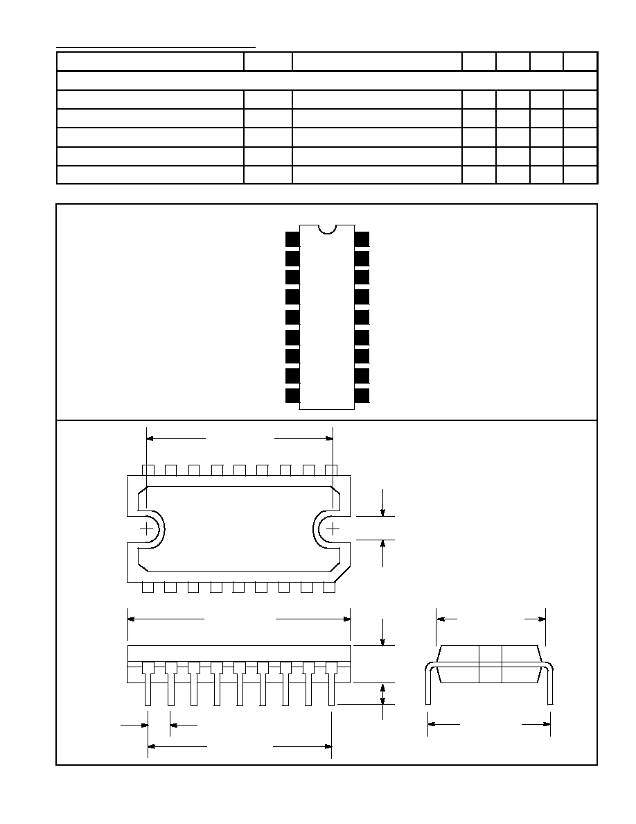
NTE1367
Integrated Circuit
Dual, Audio Power Amp, 2.3W to 5W
(4.6W to 15W BTL)
Description:
The NTE1367 is an integrated circuit in an 18≠Lead DIP type package designed for use in audio out-
put applications with low noise, low distortion and high output widely ranging for power supply and
load resistance. Two amps are built in allowing for dual or BTL operation.
Features:
D
High Output Power, Dual or BTL Operation
D
Wide Output Power Settuing Range
D
Wide Supply Voltage Range
D
Incorprated Automatic Operating Point Stabilizer Circuit
D
Low Distortion, Low 1/f Noise, and Low Shock Noise
D
High Audio Channel Separation
D
Incorporated Phase Converter
Absolute Maximum Ratings: (T
A
= +25
∞
C unless otherwise specified)
Supply Voltage, (Note 1), V
CC
20V
. . . . . . . . . . . . . . . . . . . . . . . . . . . . . . . . . . . . . . . . . . . . . . . . . . . . . . . .
Supply Current, I
CC
4A
. . . . . . . . . . . . . . . . . . . . . . . . . . . . . . . . . . . . . . . . . . . . . . . . . . . . . . . . . . . . . . . . . .
Power Dissipation (T
A
= +60
∞
C), P
D
20W
. . . . . . . . . . . . . . . . . . . . . . . . . . . . . . . . . . . . . . . . . . . . . . . . .
Operating Ambient temperature Range, T
opr
≠30
∞
to +75
∞
C
. . . . . . . . . . . . . . . . . . . . . . . . . . . . . . . . . .
Storage Temperature Range, T
stg
≠55
∞
to +150
∞
C
. . . . . . . . . . . . . . . . . . . . . . . . . . . . . . . . . . . . . . . . . .
Note 1. V
CC
at operation mode = 20V (stabilized power source).
Electrical Characteristics: (T
A
= +25
∞
C, V
CC
= 9V, Note 2 unless otherwise specified)
Parameter
Symbol
Test Conditions
Min
Typ
Max
Unit
Quiescent Circuit Current
I
CQ
V
i
= 0
20
32
55
mA
BTL (R
L
= 8
, f = 1kHz)
Voltage Gain
G
V
V
i
= 4mV
46
48
50
dB
Total Harmonic Distortion
THD
V
i
= 4mV
≠
0.4
1.0
%
Output Power
P
O
THD = 10%
4.3
4.6
≠
W
Output Noise Voltage
V
no
V
i
= 0, R
g
= 3.9k
≠
0.7
1.5
mV
Output Offset Voltage
V
O(offset)
V
i
= 0
≠100
0
+100
mV
Note 2. The value of Typ. is a reference value.
Electrical Characteristics (Cont'd): (T
A
= +25
∞
C, V
CC
= 9V, Note 2 unless otherwise specified)
Parameter
Symbol
Test Conditions
Min
Typ
Max
Unit
Dual (R
L
= 4
, f = 1kHz)
Voltage Gain
G
V
V
i
= 4mV
42
44
46
dB
Total Harmonic Distortion
THD
V
i
= 4mV
≠
0.3
1.0
%
Output Power
P
O
THD = 10%
2.0
2.3
≠
W
Output Noise Voltage
V
no
V
i
= 0, R
g
= 3.9k
≠
0.4
1.0
mV
Channel Balance
CB
V
i
= 4mV
≠
0
1
dB
Note 2. The value of Typ. is a reference value.
Electrical Characteristics: (T
A
= +25
∞
C, V
CC
= 12V, Note 2 unless otherwise specified)
Parameter
Symbol
Test Conditions
Min
Typ
Max
Unit
Quiescent Circuit Current
I
CQ
V
i
= 0
20
35
60
mA
BTL (R
L
= 8
, f = 1kHz)
Voltage Gain
G
V
V
i
= 4mV
46
48
50
dB
Total Harmonic Distortion
THD
V
i
= 4mV
≠
0.4
1.0
%
Output Power
P
O
THD = 10%
7.5
8.3
≠
W
Output Noise Voltage
V
no
V
i
= 0, R
g
= 10k
≠
0.7
2.0
mV
Output Offset Voltage
V
O(offset)
V
i
= 0
≠100
0
+100
mV
Dual (R
L
= 4
, f = 1kHz)
Voltage Gain
G
V
V
i
= 4mV
42
44
46
dB
Total Harmonic Distortion
THD
V
i
= 4mV
≠
0.3
1.0
%
Output Power
P
O
THD = 10%
3.6
4.0
≠
W
Output Noise Voltage
V
no
V
i
= 0, R
g
= 3.9k
≠
0.5
1.5
mV
Channel Balance
CB
V
i
= 4mV
≠
0
1
dB
Note 2. The value of Typ. is a reference value.
Electrical Characteristics: (T
A
= +25
∞
C, V
CC
= 13.2V, Note 2 unless otherwise specified)
Parameter
Symbol
Test Conditions
Min
Typ
Max
Unit
Quiescent Circuit Current
I
CQ
V
i
= 0
20
38
60
mA
BTL (R
L
= 8
, f = 1kHz)
Voltage Gain
G
V
V
i
= 4mV
46
48
50
dB
Total Harmonic Distortion
THD
V
i
= 4mV
≠
0.4
1.0
%
Output Power
P
O
THD = 10%
9.4
10
≠
W
Output Noise Voltage
V
no
V
i
= 0, R
g
= 10k
≠
0.7
2.0
mV
Output Offset Voltage
V
O(offset)
V
i
= 0
≠100
0
+100
mV
Note 2. The value of Typ. is a reference value.