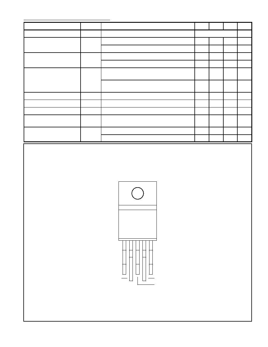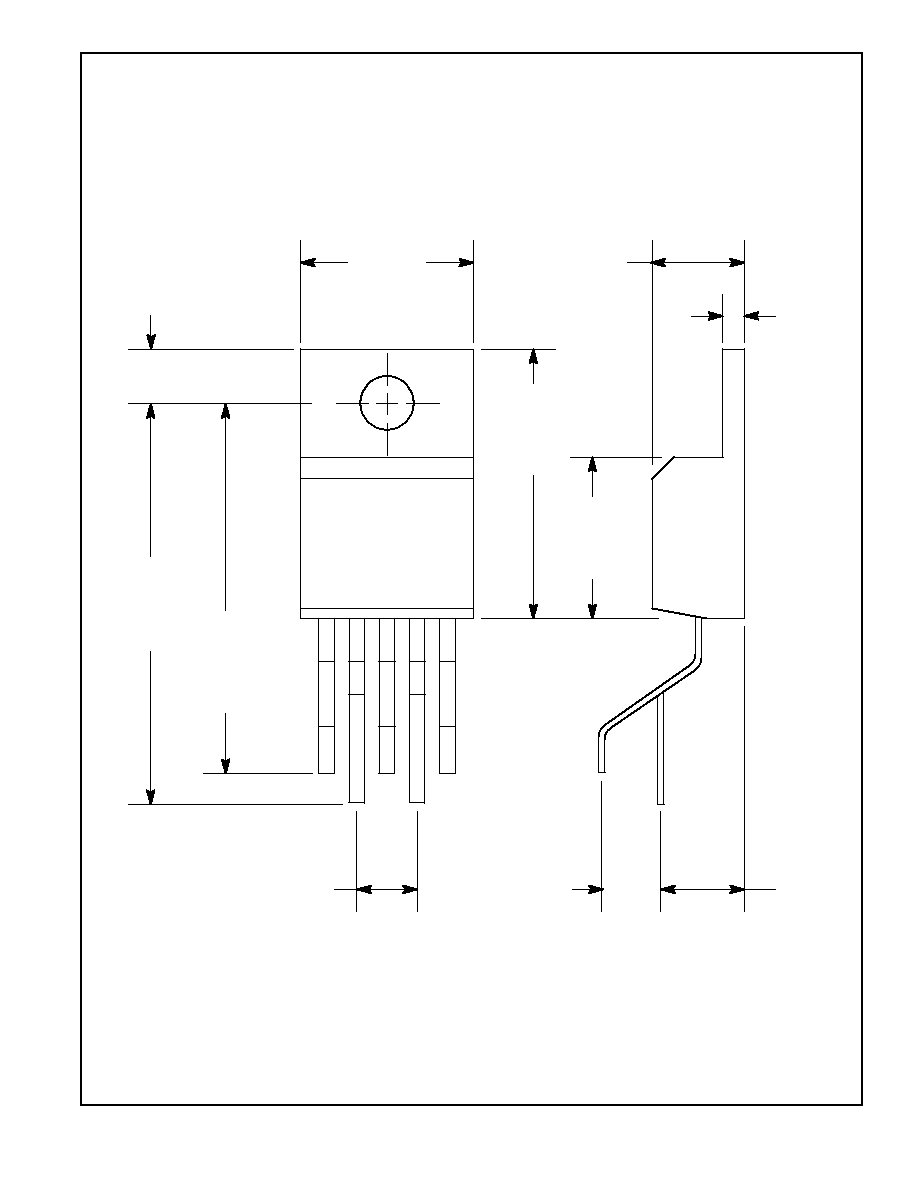
NTE1380
Integrated Circuit
Audio Power Amplifier, 14W
Description:
The NTE1380 is a monolithic integrated circuit in a 5≠Lead TO220 type package intended for use as
an audio class AB amplifier. Typically, it provides 14W output power (THD = 0.5%) at V
S
=
±
14V/4
.
This device provides high output current and has very low harmonic and cross≠over distortion. Fur-
ther, the NTE1380 incorporates a short circuit protection system comprising an arrangement for auto-
matically limiting the dissipated power so as to keep the working point of the output transistors within
their safe operating area. A thermal shut≠down system is also included.
Absolute Maximum Ratings:
Supply Voltage, V
S
±
18V
. . . . . . . . . . . . . . . . . . . . . . . . . . . . . . . . . . . . . . . . . . . . . . . . . . . . . . . . . . . . . . . .
Input Voltage, V
I
V
S
. . . . . . . . . . . . . . . . . . . . . . . . . . . . . . . . . . . . . . . . . . . . . . . . . . . . . . . . . . . . . . . . . . . .
Differential Input Voltage, V
I
±
15V
. . . . . . . . . . . . . . . . . . . . . . . . . . . . . . . . . . . . . . . . . . . . . . . . . . . . . . . .
Output Peak Current (Internally Limited), I
O
3.5A
. . . . . . . . . . . . . . . . . . . . . . . . . . . . . . . . . . . . . . . . . . .
Power Dissipation (T
C
= +90
∞
C), P
tot
20W
. . . . . . . . . . . . . . . . . . . . . . . . . . . . . . . . . . . . . . . . . . . . . . . . .
Operating Junction Temperature Range, T
J
≠40
∞
to +150
∞
C
. . . . . . . . . . . . . . . . . . . . . . . . . . . . . . . . . .
Storage Temperature Range, T
stg
≠40
∞
to +150
∞
C
. . . . . . . . . . . . . . . . . . . . . . . . . . . . . . . . . . . . . . . . . .
Thermal Resistance, Junction≠to≠Case, R
thJC
3
∞
C/W
. . . . . . . . . . . . . . . . . . . . . . . . . . . . . . . . . . . . . . .
Min. Thermal Shut≠Down Junction Temperature (V
S
=
±
14V, P
tot
= 12W, T
A
= +25
∞
C), T
sd
+110
∞
C
Electrical Characteristics: (V
S
=
±
14V, T
A
= +25
∞
C unless otherwise specified)
Parameter
Symbol
Test Conditions
Min
Typ
Max
Unit
Supply Voltage
V
S
±
6
≠
±
18
V
Quiescent Drain Current
I
d
V
S
=
±
18V
≠
40
60
mA
Input Bias Current
I
b
V
S
=
±
18V
≠
0.2
2.0
µ
A
Input Offset Voltage
V
OS
V
S
=
±
18V
≠
±
2
±
20
mV
Input Offset Current
I
OS
V
S
=
±
18V
≠
±
20
±
200
nA
Output Offset Voltage
V
OS
V
S
=
±
18V
≠
±
2.5
±
22
mV
Output Power
P
O
THD = 0.5%, G
V
= 30dB, f = 40 to 15000Hz,
R
L
= 4
12
14
≠
W
THD = 0.5%, G
V
= 30dB, f = 40 to 15000Hz,
R
L
= 8
8
9
≠
W
THD = 10%, G
V
= 30dB, f = 1kHz, R
L
= 4
≠
18
≠
W
THD = 10%, G
V
= 30dB, f = 1kHz, R
L
= 8
≠
11
≠
W