NTE162
Silicon NPN Transistor
TV Vertical Deflection
Description:
The NTE162 is an NPN transistor in a TO3 type case designed for mediumÙtoÙhigh voltage inverters,
converters, regulators, and switching circuits.
Features:
D
High Voltage: V
CEX
= 400V
D
Gain Specified to 3.5A
D
High Frequency Response to 2.5MHz
Absolute Maximum Ratings:
CollectorÙEmitter Voltage, V
CEX
400V
. . . . . . . . . . . . . . . . . . . . . . . . . . . . . . . . . . . . . . . . . . . . . . . . . . . . .
CollectorÙBase Voltage, V
CB
400V
. . . . . . . . . . . . . . . . . . . . . . . . . . . . . . . . . . . . . . . . . . . . . . . . . . . . . . . .
EmitterÙBase Voltage, V
EBO
5V
. . . . . . . . . . . . . . . . . . . . . . . . . . . . . . . . . . . . . . . . . . . . . . . . . . . . . . . . . .
Continuous Collector Current, I
C
10A
. . . . . . . . . . . . . . . . . . . . . . . . . . . . . . . . . . . . . . . . . . . . . . . . . . . . .
Base Current, I
B
2A
. . . . . . . . . . . . . . . . . . . . . . . . . . . . . . . . . . . . . . . . . . . . . . . . . . . . . . . . . . . . . . . . . . . .
Total Device Dissipation (T
C
= +25
¯
C), P
D
125W
. . . . . . . . . . . . . . . . . . . . . . . . . . . . . . . . . . . . . . . . . . .
Derate Above 25
¯
C
1W/
¯
C
. . . . . . . . . . . . . . . . . . . . . . . . . . . . . . . . . . . . . . . . . . . . . . . . . . . . . . . . .
Operating Junction Temperature Range, T
J
Ù65
¯
to +150
¯
C
. . . . . . . . . . . . . . . . . . . . . . . . . . . . . . . . . .
Storage Temperature Range, T
stg
Ù65
¯
to +200
¯
C
. . . . . . . . . . . . . . . . . . . . . . . . . . . . . . . . . . . . . . . . . .
Thermal Resistance, JunctionÙtoÙCase, R
thJC
1
¯
C/W
. . . . . . . . . . . . . . . . . . . . . . . . . . . . . . . . . . . . . . .
Electrical Characteristics: (T
A
= +25
¯
C unless otherwise specified)
Parameter
Symbol
Test Conditions
Min
Typ
Max Unit
OFF Characteristics
CollectorÙEmitter Sustaining Voltage
V
(BR)CEO(sus)
I
C
= 100mA, I
B
= 0, Note 1
325
Ù
Ù
V
Collector Cutoff Current
I
CEX
V
CE
= 400V, V
EB(off)
= 1.5V
Ù
Ù
2.5
mA
V
CE
= 400V, V
EB(off)
= 1.5V,
T
C
= +125
¯
C
Ù
Ù
1.0
mA
Emitter Cutoff Current
I
EBO
V
BE
= 5V, I
C
= 0
Ù
Ù
2.0
mA
Note 1. Pulse Test: Pulse Width
300
ç
s, Duty Cycle
2%.
Electrical Characteristics (Cont'd): (T
A
= +25
¯
C unless otherwise specified)
Parameter
Symbol
Test Conditions
Min
Typ
Max Unit
ON Characteristics (Note 1)
DC Current Gain
h
FE
I
C
= 2.5A, V
CE
= 5V
15
Ù
35
I
C
= 3.5A, V
CE
= 5V
10
Ù
Ù
CollectorÙEmitter Saturation Voltage
V
CE(sat)
I
C
= 2.5A, I
B
= 0.5A
Ù
Ù
0.7
V
BaseÙEmitter Saturation Voltage
V
BE(sat)
I
C
= 2.5A, I
B
= 0.5A
Ù
Ù
1.5
V
Dynamic Characteristics
Current GainÙBandwidth Product
f
T
I
C
= 200mA, V
CE
= 10V, f = 1MHz
2.5
Ù
Ù
MHz
Note 1. Pulse Test: Pulse Width
300
ç
s, Duty Cycle
2%.
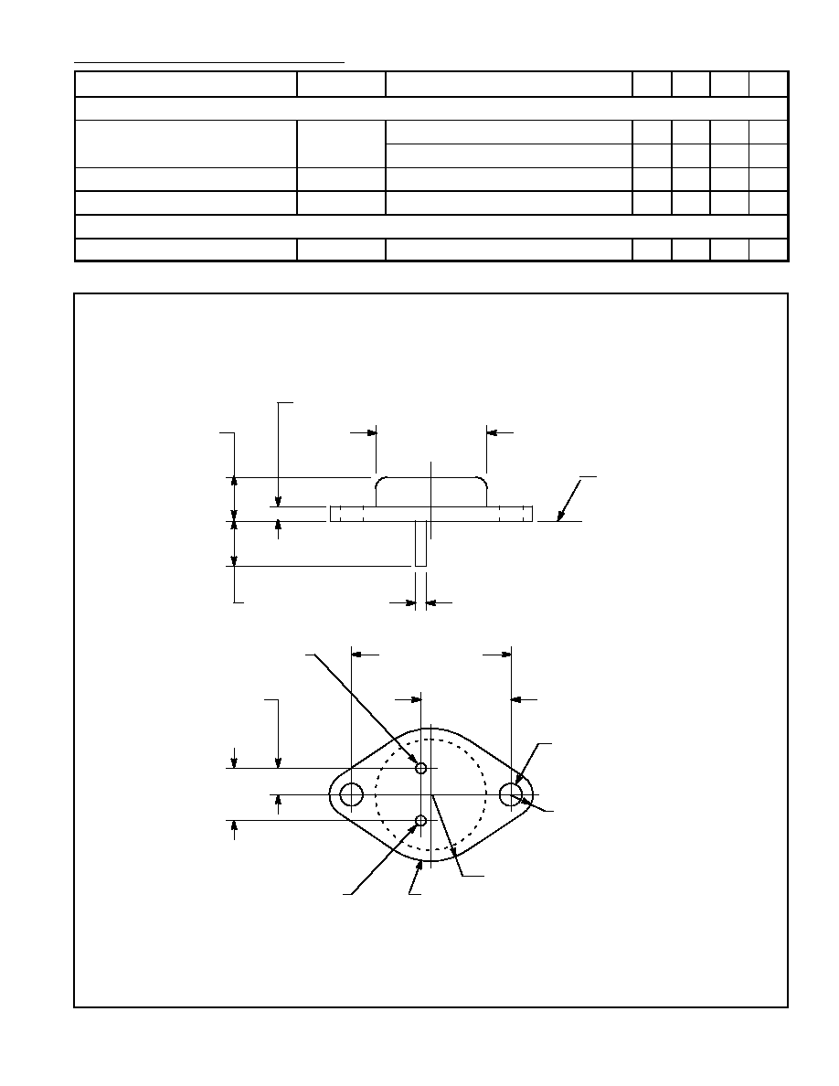
1.187 (30.16)
.875 (22.2)
Dia Max
.665
(16.9)
.430
(10.92)
Seating
Plane
.040 (1.02)
.312 (7.93) Min
.135 (3.45) Max
.350 (8.89)
Emitter
Collector/Case
Base
.215 (5.45)
.525 (13.35) R Max
.156 (3.96) Dia
(2 Holes)
.188 (4.8) R Max