NTE5498 & NTE5499
Silicon Controlled Rectifier (SCR)
12 Amp
Description:
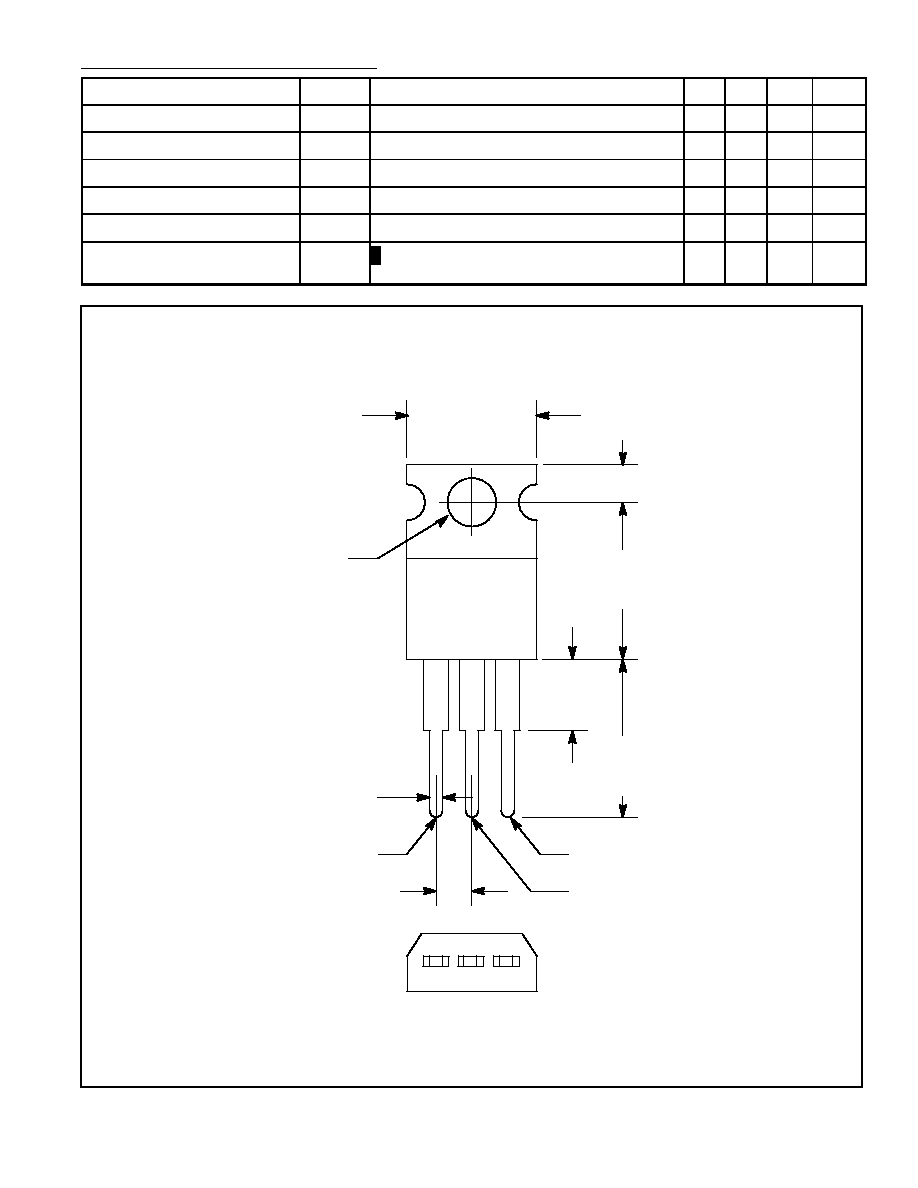
The NTE5498 and NTE5499 silicon controlled rectifiers are high performance glass passivated
PNPN devices in a TO220 type package designed for general purpose high current applications
where moderate gate sensitivity is required.
Absolute Maximum Ratings: (T
A
= +25
∞
C unless otherwise specified)
Peak Repetitive Off≠State Voltage (T
J
= ≠40
∞
to +125
∞
C, R
GK
= 1k
), V
DRM
, V
RRM
NTE5498
400V
. . . . . . . . . . . . . . . . . . . . . . . . . . . . . . . . . . . . . . . . . . . . . . . . . . . . . . . . . . . . . . . . . . .
NTE5499
800V
. . . . . . . . . . . . . . . . . . . . . . . . . . . . . . . . . . . . . . . . . . . . . . . . . . . . . . . . . . . . . . . . . . .
RMS On≠State Current (All Conduction Angles, T
C
= +85
∞
C), I
T(RMS)
12A
. . . . . . . . . . . . . . . . . . . . .
Average On≠State Current (Half Cycle, 180
∞
Conduction Angle, T
C
= +85
∞
C), I
T(AV)
7.6A
. . . . . . . .
Non≠Repetitive On≠State Current (Half Cycle, 60Hz), I
TSM
132A
. . . . . . . . . . . . . . . . . . . . . . . . . . . . .
Non≠Repetitive On≠State Current (Half Cycle, 50Hz), I
TSM
120A
. . . . . . . . . . . . . . . . . . . . . . . . . . . . .
Circuit Fusing Considerations (Half Cycle, t = 10ms), I
2
t
72A
2
s
. . . . . . . . . . . . . . . . . . . . . . . . . . . . . . .
Peak Gate Current (10
µ
s Max), I
GM
4A
. . . . . . . . . . . . . . . . . . . . . . . . . . . . . . . . . . . . . . . . . . . . . . . . . . .
Peak Gate Dissipation (10
µ
s Max), P
GM
10W
. . . . . . . . . . . . . . . . . . . . . . . . . . . . . . . . . . . . . . . . . . . . . .
Average Gate Dissipation (20ms Max), P
G(AV)
1W
. . . . . . . . . . . . . . . . . . . . . . . . . . . . . . . . . . . . . . . . .
Operating Junction Temperature Range, T
J
≠40
∞
to +125
∞
C
. . . . . . . . . . . . . . . . . . . . . . . . . . . . . . . . . .
Storage Temperature Range, T
stg
≠40
∞
to +125
∞
C
. . . . . . . . . . . . . . . . . . . . . . . . . . . . . . . . . . . . . . . . . .
Thermal Resistance, Junction≠to≠Case, R
thJC
3K/W
. . . . . . . . . . . . . . . . . . . . . . . . . . . . . . . . . . . . . . .
Thermal Resistance, Junction≠to≠Ambient, R
thJA
60K/W
. . . . . . . . . . . . . . . . . . . . . . . . . . . . . . . . . . . .
Lead Temperature (During Soldering, 1.6mm from case, 10sec max), T
L
+250
∞
C
. . . . . . . . . . . . . . .
Electrical Characteristics: (T
A
= +25
∞
C unless otherwise specified)
Parameter
Symbol
Test Conditions
Min Typ Max
Unit
Off≠State Leakage Current
I
DRM
,
V
DRM
+ V
RRM
, R
GK
= 1k
T
J
= +125
∞
C
≠
≠
1.5
mA
I
RRM
T
J
= +25
∞
C
≠
≠
5.0
µ
A
On≠State Voltage
V
T
I
T
= 24A, T
J
= +25
∞
C
≠
≠
1.8
V
On≠State Threshold Voltage
V
T(TO)
T
J
= +125
∞
C
≠
≠
1.0
V
On≠State Slope Resistance
r
T
T
J
= +125
∞
C
≠
≠
36
m
Gate≠Trigger Current
I
GT
V
D
= 7V
5
≠
10
mA
Gate≠Trigger Voltage
V
GT
V
D
= 7V
≠
≠
2.0
V