NTE1808
Integrated Circuit
Playback Video Processor for VCR
Description:
The NTE1808 is a integrated circuit in a 28≠Lead DIP type package designed for VCR playback video
signal processin circuits.
Features:
D
Built≠In Line Noise Canceler
D
Built≠In Picture Control Circuit
D
Supply Voltage: V
CC
= 5V
Absolute Maximum Ratings: (T
A
= +25
∞
C unless otherwise specified)
Supply Voltage, V
CC
6V
. . . . . . . . . . . . . . . . . . . . . . . . . . . . . . . . . . . . . . . . . . . . . . . . . . . . . . . . . . . . . . . . .
Power Dissipation (T
A
= +70
∞
C), P
D
200mW
. . . . . . . . . . . . . . . . . . . . . . . . . . . . . . . . . . . . . . . . . . . . . .
Operating Ambient Temperature Range, T
opr
≠20
∞
to +70
∞
C
. . . . . . . . . . . . . . . . . . . . . . . . . . . . . . . . . .
Storage Temperature Range, T
stg
≠55
∞
to +150
∞
C
. . . . . . . . . . . . . . . . . . . . . . . . . . . . . . . . . . . . . . . . . .
Electrical Characteristics: (V
CC
= 5V, T
A
= +25
∞
C unless otherwise specified)
Parameter
Symbol
Test Conditions
Min
Typ
Max
Unit
Circuit Current
I
23
17
≠
30
mA
DOC Amplifier Gain
G
25
Pin24 Input (60mV
P≠P
, 4MHz)
13
≠
16
dB
DOC Sensitivity ON
S
28
Pin26 Input (4MHz), 0dB = 350mV
P≠P
≠15
≠
≠11.5
dB
DOC Sensitivity OFF (Hysteresis)
D
S
28
≠5
≠
≠0.5
dB
Sub FM Demodulation Det.
Sensitivity
S
15
Pin24 Input (50mV
P≠P
) Pin17 3.5V
F11 is multiplied by Gain (0dB = 250mV)
2.5
≠
≠
dB
Sub FM Demodulation Det.
Limitation
L
f15
Pin24 Input (100mV
P≠P
), Pin17 3.5V
7
≠
≠
MHz
Main FM Demodulation Det.
Sensitivity
S
16
Pin21 Input (150mV
P≠P
), Pin17 3.5V
F11 is multiplied by Gain (0dB = 250mV)
2.5
≠
≠
dB
Main FM Demodulation Det.
Limitation
L
f16
Pin21 Input (100mV
P≠P
), Pin17 3.5V
7
≠
≠
MHz
Difference Det. Amp. Gain A
G
11≠1
Pin14 Input (100mV
P≠P
, 1MHz)
13.5
≠
16.5
dB
Difference Det. Amp. Gain B
G
11≠2
Pin13 Input (100mV
P≠P
, 1MHz)
12
≠
15
dB
Note 1. Operating Supply Voltage Range: V
CC(opr)
= 4.5V to 5.5V
Electrical Characteristics (Cont'd): (V
CC
= 5V, T
A
= +25
∞
C unless otherwise specified)
Parameter
Symbol
Test Conditions
Min
Typ
Max
Unit
Differential + Mix Amp Gain
G
4≠1
7
≠
10
dB
Mix Amp. Ratio
G
4≠2
Pin12 Input (500mV
P≠P
, 1MHz)
≠5.5
≠
≠2.5
dB
Line Noise Canceler Switch
Changeover Level Difference
Du
4
Pin27 Control Pulse
≠5
≠
5
mV
Line Noise Canceler Switch
Crosstalk
CT
4
500mV
P≠P
, 1MHz Pin4 Output Ratio of
Pin10 & Pin12
≠
≠
≠40
dB
Line Noise Canceler Limiter Gain
G
7
Pin9 Input (40mV
P≠P
, 1MHz)
15.5
≠
19.0
dB
Line Noise Canceler Cerrlative
Det. Sensitivity ON
S
6
Pin9 Input (4MHz), 0dB = 60mV
P≠P
1.5
≠
4.5
dB
Line Noise Canceler Cerrlative
Det. Sensitivity OFF (Hysteresis)
D
S
6
Pin9 Input (4MHz), 0dB = 60mV
P≠P
≠4
≠
≠0.1
dB
Picture Gain Control
G
1
Pin3 Input (250mV
P≠P
, 1MHz), Output
Ratio of Pin2 0V and 2.5V
≠1.5
≠
0.5
dB
Picture Control Frequency
Characteristics A
f
1≠1
Pin3 Input (250mV
P≠P
, 1MHz)
≠
≠
≠3
dB
Picture Control Frequency
Characteristics B
f
1≠2
Pin3 Input (250mV
P≠P
, 1MHz), Output
Ratio of Pin2 5V and 2.5V
5
≠
≠
dB
Note 1. Operating Supply Voltage Range: V
CC(opr)
= 4.5V to 5.5V
Note 2. Pin8 shall be always used in connection with Pin23
Note 3. Power supply to be supplied to the variable resistor added to Pin2 and Pin17 shall be used
the same as that supplied to this integrated circuit.
Note 4. Since deterioration or destroy of characteristics due to flow of overcurrent caused by reverse
current, careful should be taken to handling.
V
CC
V
CC
(Record)
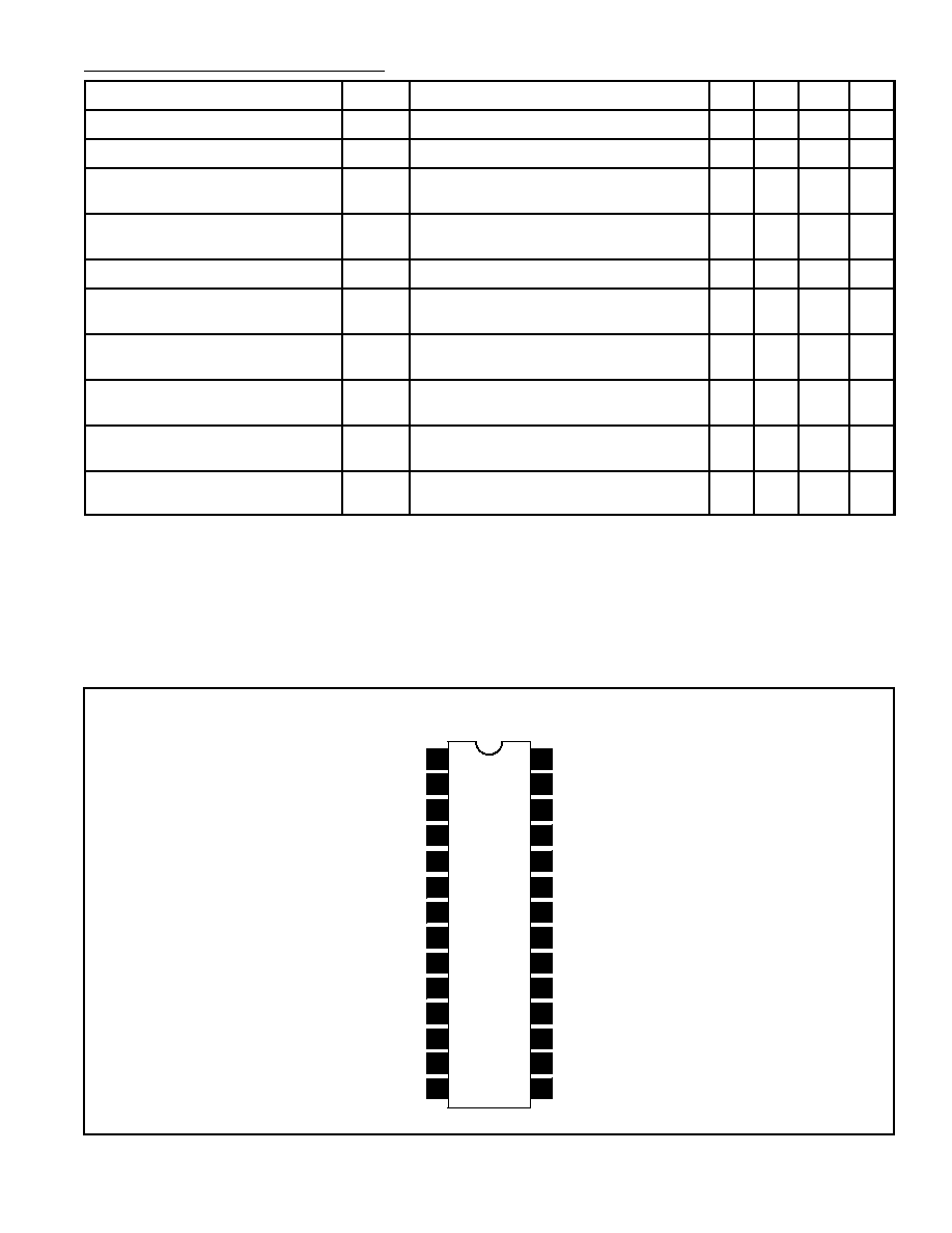
Pin Connection Diagram
RF Output
Envelope DET
Video Output
GND
Extension
Peaking
Diff Signal Output
1H Delay RF Input
RF Input
Limited Signal Input
Double LIM H.P.F. Input
1
2
3
4
Picture Control
De≠Emphasis
5
6
Relative Detecting Pulse Output
7
Line N.C. LIM Output
8
28
27
26
25
DOC Pulse Output
24
23
22
21
9
Line N.C. LIM Input
20
LIM
LIM
10
Diff Signal Input
11
19
18
DEM Gain Control
12
17
DEM Output
13
Video Input
16
14
Video (1H DL) Input
15
DEM (1H DL) Output
Double LIM H.P.F. Input