NTE2021 & NTE2022
Integrated Circuit
8≠Digit/Segment Fluorescent Display Driver
Description:
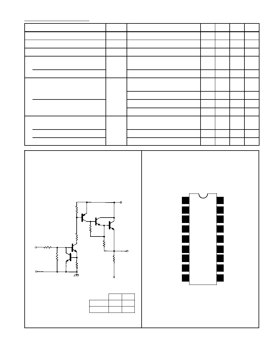
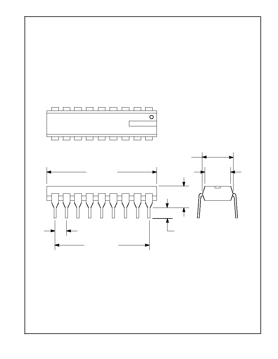
The NTE2021 and NTE2022 consist of eight NPN Darlington output stages and the associated com-
mon≠emitter input stages in an 18≠Lead DIP type package. These devices are designed to interface
between low≠level digital logic and vacuum fluorescent displays. They are capable of driving the dig-
its and/or segments of these displays and are designed to permit all outputs to be activated simulta-
neously. Pulldown resistors are incorporated into each output and no external components are re-
quired for most fluorescent displays.
The NTE2020 is compatible with TTL, Schottky TTL, DTL and 5V CMOS. The NTE2021 device is
intended for use with MOS (PMOS & CMOS) logic operating from supply voltages of 6V to 15V.
Features:
D
Digit or Segment Drivers
D
Low Input Current
D
Integral Output Pull≠Down Resistors
D
Low Power
D
Reliable Monolithic Construction
D
High Output Breakdown Voltage
Absolute Maximum Ratings: (T
A
= +25
∞
C, Note 1)
Supply Voltage, V
BB
85V
. . . . . . . . . . . . . . . . . . . . . . . . . . . . . . . . . . . . . . . . . . . . . . . . . . . . . . . . . . . . . . . .
Input Voltage, V
IN
20V
. . . . . . . . . . . . . . . . . . . . . . . . . . . . . . . . . . . . . . . . . . . . . . . . . . . . . . . . . . . . . . . . . .
Output Current, I
OUT
≠40mA
. . . . . . . . . . . . . . . . . . . . . . . . . . . . . . . . . . . . . . . . . . . . . . . . . . . . . . . . . . . . .
Allowable Power Dissipation, P
D
1W
. . . . . . . . . . . . . . . . . . . . . . . . . . . . . . . . . . . . . . . . . . . . . . . . . . . . .
Derate Above 25
∞
C
8.0mW/
∞
C
. . . . . . . . . . . . . . . . . . . . . . . . . . . . . . . . . . . . . . . . . . . . . . . . . . . . .
Operating Temperature Range, T
A
≠20
∞
to +85
∞
C
. . . . . . . . . . . . . . . . . . . . . . . . . . . . . . . . . . . . . . . . . . .
Storage Temperature Range, T
stg
≠55
∞
to +150
∞
C
. . . . . . . . . . . . . . . . . . . . . . . . . . . . . . . . . . . . . . . . . .
Note 1. Voltages are with reference to GND unless otherwise specified
Recommended Operating Conditions:
Parameter
Symbol
Test Conditions
Min
Typ
Max
Unit
Supply Voltage
V
BB
5
≠
70
V
Input ON Voltage
NTE2021
V
IN
2.4
≠
15
V
NTE2022
4.0
≠
15
V
Output ON Current
I
OUT
≠
≠
≠25
mA
Note 2. Positive (negative) current is defined as going into (coming out of) the specified device pin.